
مراجعة بنية الطبقات والمستويات المرجعية والحفر الخلفي للوحات عالية البيانات. نطاق العملية الموثق: Impedance tolerance: ±8%; Back drilling: Any-layer capability; Mechanical aspect ratio: Up to 20:1 ملفات المراجعة: Gerber أو ODB++ وملفات الحفر وبنية الطبقات والرسم والكمية والموعد المطلوب. الحدود المنشورة مأخوذة من جدول قدرات JETFGO الحالي، وتتطلب الجدوى النهائية حزمة بيانات كاملة.
الحدود المنشورة مأخوذة من جدول قدرات JETFGO الحالي، وتتطلب الجدوى النهائية حزمة بيانات كاملة.رمز الحلHS-06Lقدرة موثقة
PCB عالية السرعة بست طبقات
مراجعة بنية الطبقات والمستويات المرجعية والحفر الخلفي للوحات عالية البيانات.
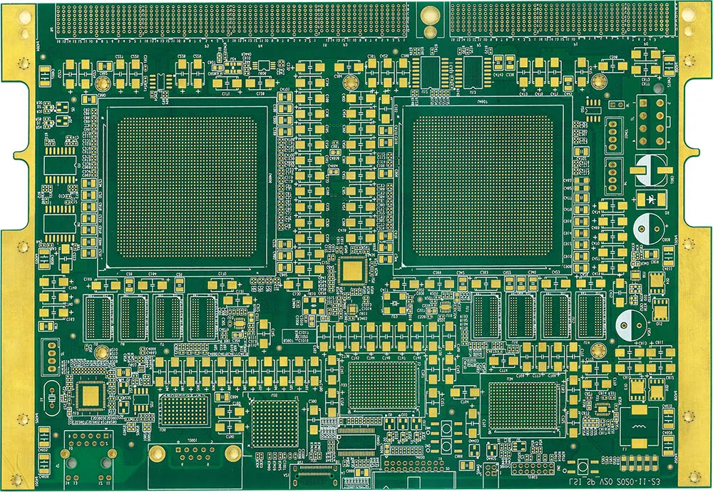
JETFGO / HS-06LRIGID
01 / الإجابة الهندسية
الإجابة الهندسية
02 / DATA
نطاق العملية الموثق
مراجعة بنية الطبقات والمستويات المرجعية والحفر الخلفي للوحات عالية البيانات.
Impedance Tolerance
±8%
Back Drilling
Target-layer and depth review based on stack-up
Mechanical Aspect Ratio
Up to 20:1
High-Speed Stack-up
Reference-plane and controlled-impedance review
Back-Drill Review
Drill side · target layer · residual stub · depth
05 / INPUT
ملفات المراجعة
High-Speed PCB Engineering Package
Gerber or ODB++, drill files, proposed stack-up, fabrication drawing, quantity, target delivery date and applicable controlled-impedance or back-drill requirements.
Controlled-Impedance Requirements
Provide target impedance, tolerance, routing layer, reference plane and applicable single-ended or differential signal classes.
Back-Drill Requirements
Provide the required drill side, target layer, residual stub requirement and any project-specific back-drill depth or tolerance information.
High-Speed Stack-up
اطلب عرض سعرProvide the proposed layer order, signal layers, reference planes, board thickness, copper requirements and material preferences when available.
06 / FAQ
أسئلة تقنية
الحدود المنشورة مأخوذة من جدول قدرات JETFGO الحالي، وتتطلب الجدوى النهائية حزمة بيانات كاملة.
01Is ±8% impedance tolerance guaranteed for every 6-layer high-speed PCB?+
No. ±8% is a published capability reference for this solution. Final impedance feasibility depends on the complete stack-up, materials, dielectric structure, copper thickness, trace geometry and target impedance confirmed during engineering review.
02Which files help JETFGO review a 6-layer high-speed PCB fastest?+
Send Gerber or ODB++, drill files, proposed stack-up, fabrication drawing, quantity, target delivery date and any controlled-impedance or back-drill requirements.
03Can JETFGO support prototypes and repeat production for 6-layer high-speed PCBs?+
Yes. Once the stack-up, materials, impedance requirements and back-drill conditions are confirmed, the approved engineering record can support prototype validation and repeat production under the same manufacturing conditions.
04Why is stack-up important for a 6-layer high-speed PCB?+
The stack-up defines the relationship between signal layers, reference planes, dielectric thickness and copper geometry. These factors directly affect controlled impedance, return-current paths and high-speed signal integrity.
05When is back drilling needed on a high-speed PCB?+
Back drilling may be considered when unused plated-through-hole stubs could affect high-speed signal integrity. Final need and drill depth depend on the signal requirements, stack-up, via transitions and acceptable residual stub.
06What is a via stub in a high-speed PCB?+
A via stub is the unused conductive portion of a plated through-hole beyond the signal connection layer. At high data rates, it can contribute to reflections and impedance discontinuities, so selected vias may require back drilling.
07Can a 6-layer PCB support both single-ended and differential impedance?+
Yes. A 6-layer PCB can support single-ended and differential controlled-impedance signals when the stack-up, routing layers, reference planes and trace geometry are designed appropriately and confirmed during engineering review.
RFQ / DFM
أرسل المتطلبات واحصل على خطة توريد قابلة للتنفيذ.
أرسل Gerber أو ODB++ والطبقات والمواد والكمية والموعد والاختبارات لمراجعة القابلية وتقديم عرض فني.
مراجعة هندسيةالمواد والبنيةتصنيع دقيق