
Revisione di stack-up, piani di riferimento e back-drill per schede ad alta velocità. Finestra di processo verificata: Impedance tolerance: ±8%; Back drilling: Any-layer capability; Mechanical aspect ratio: Up to 20:1 File per la revisione: Gerber o ODB++, file di foratura, stack-up, disegno, quantità e data richiesta. I limiti pubblicati derivano dall’attuale tabella capacità JETFGO; la fattibilità finale richiede i dati completi.
I limiti pubblicati derivano dall’attuale tabella capacità JETFGO; la fattibilità finale richiede i dati completi.Codice soluzioneHS-06LCapacità verificata
PCB high-speed a 6 strati
Revisione di stack-up, piani di riferimento e back-drill per schede ad alta velocità.
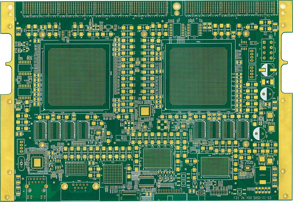
JETFGO / HS-06LRIGID
01 / RISPOSTA TECNICA
Risposta tecnica
02 / DATA
Finestra di processo verificata
Revisione di stack-up, piani di riferimento e back-drill per schede ad alta velocità.
Impedance Tolerance
±8%
Back Drilling
Target-layer and depth review based on stack-up
Mechanical Aspect Ratio
Up to 20:1
High-Speed Stack-up
Reference-plane and controlled-impedance review
Back-Drill Review
Drill side · target layer · residual stub · depth
05 / INPUT
File per la revisione
High-Speed PCB Engineering Package
Gerber or ODB++, drill files, proposed stack-up, fabrication drawing, quantity, target delivery date and applicable controlled-impedance or back-drill requirements.
Controlled-Impedance Requirements
Provide target impedance, tolerance, routing layer, reference plane and applicable single-ended or differential signal classes.
Back-Drill Requirements
Provide the required drill side, target layer, residual stub requirement and any project-specific back-drill depth or tolerance information.
High-Speed Stack-up
Richiedi un preventivoProvide the proposed layer order, signal layers, reference planes, board thickness, copper requirements and material preferences when available.
06 / FAQ
Domande tecniche
I limiti pubblicati derivano dall’attuale tabella capacità JETFGO; la fattibilità finale richiede i dati completi.
01Is ±8% impedance tolerance guaranteed for every 6-layer high-speed PCB?+
No. ±8% is a published capability reference for this solution. Final impedance feasibility depends on the complete stack-up, materials, dielectric structure, copper thickness, trace geometry and target impedance confirmed during engineering review.
02Which files help JETFGO review a 6-layer high-speed PCB fastest?+
Send Gerber or ODB++, drill files, proposed stack-up, fabrication drawing, quantity, target delivery date and any controlled-impedance or back-drill requirements.
03Can JETFGO support prototypes and repeat production for 6-layer high-speed PCBs?+
Yes. Once the stack-up, materials, impedance requirements and back-drill conditions are confirmed, the approved engineering record can support prototype validation and repeat production under the same manufacturing conditions.
04Why is stack-up important for a 6-layer high-speed PCB?+
The stack-up defines the relationship between signal layers, reference planes, dielectric thickness and copper geometry. These factors directly affect controlled impedance, return-current paths and high-speed signal integrity.
05When is back drilling needed on a high-speed PCB?+
Back drilling may be considered when unused plated-through-hole stubs could affect high-speed signal integrity. Final need and drill depth depend on the signal requirements, stack-up, via transitions and acceptable residual stub.
06What is a via stub in a high-speed PCB?+
A via stub is the unused conductive portion of a plated through-hole beyond the signal connection layer. At high data rates, it can contribute to reflections and impedance discontinuities, so selected vias may require back drilling.
07Can a 6-layer PCB support both single-ended and differential impedance?+
Yes. A 6-layer PCB can support single-ended and differential controlled-impedance signals when the stack-up, routing layers, reference planes and trace geometry are designed appropriately and confirmed during engineering review.
RFQ / DFM
Invia il requisito. Ricevi un piano di fornitura producibile.
Invia Gerber o ODB++, stackup, materiali, quantità, data richiesta e test per la verifica tecnica e il preventivo.
Revisione tecnicaMateriali e stack-upFabbricazione