
Intelligenza produttiva
Capacità di produzione PCB
Parametri trasparenti per PCB multistrato, HDI, high-speed, RF e rigid-flex.
Preventivo diretto dal produttoreJETFGO / Capacità di produzione PCB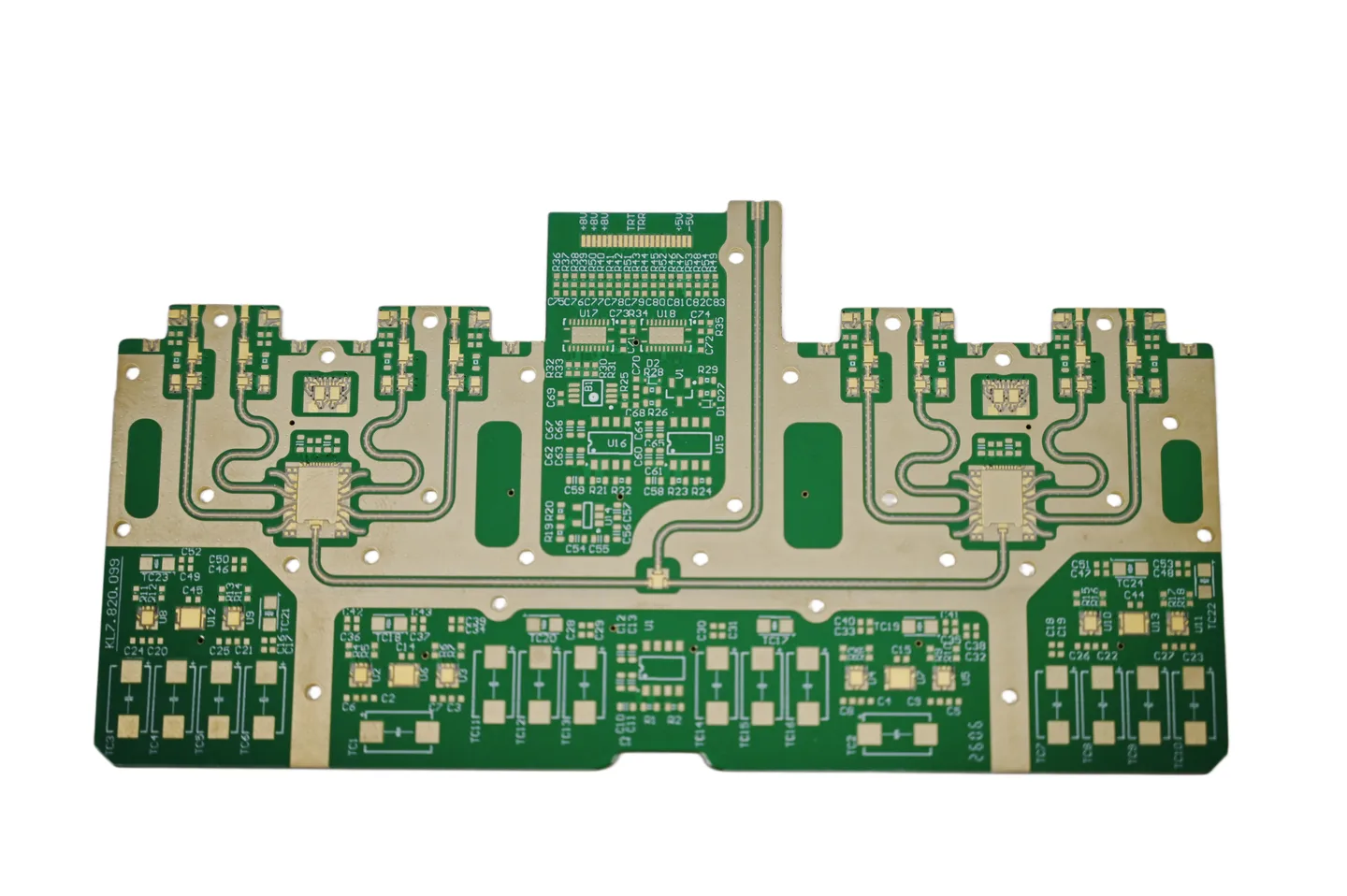 PRODUCT & PROCESS DETAIL
TECHNICAL WINDOW
Precisione specificabile. Qualità verificabile.
Processi controllati e ispezioni rigorose trasformano dati complessi in produzione ripetibile.
EXTENDED PORTFOLIO
Precisione specificabile. Qualità verificabile.
Parametri trasparenti per PCB multistrato, HDI, high-speed, RF e rigid-flex.
07
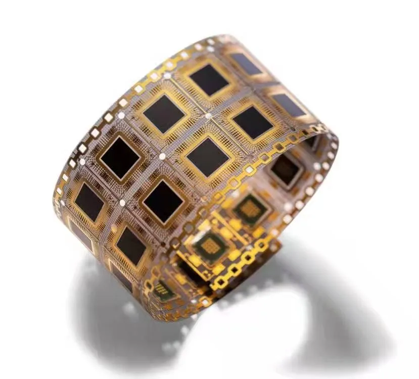
Circuiti stampati flessibili
Circuiti flessibili a geometria fine con produzione in fogli o roll-to-roll.
Dettagli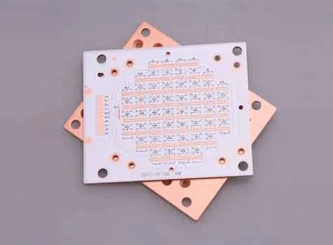
08
PCB a base metallica
Strutture in alluminio, rame e metalli speciali per progetti termici e di potenza.
Dettagli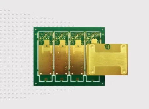
10
Inserto in rame PCB Produttore
Inserto in rame PCB produzione con inserti in rame incorporati per la gestione termica diretta in applicazioni elettroniche ad alta potenza, automobilistiche e industriali.
Dettagli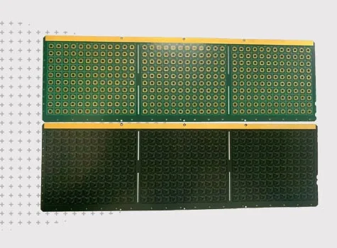
11
PCB tipo substrato SLP
Interconnessioni any-layer a linea fine per moduli compatti, previa revisione tecnica.
Dettagli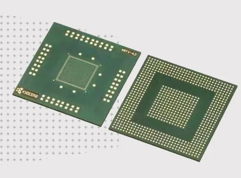
12
Substrato IC ABF
Substrati package ABF ultrafini per interconnessioni avanzate, previa revisione tecnica.
Dettagli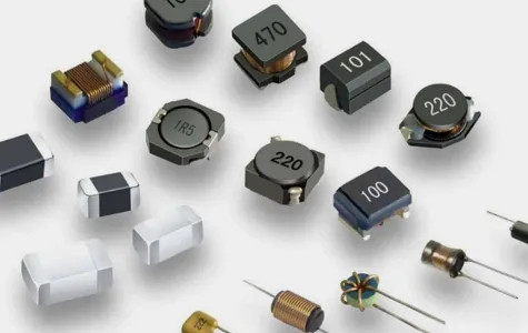
15
Approvvigionamento componenti
Acquisto da BOM, verifica della tracciabilità e coordinamento della fornitura per PCBA.
DettagliCAPACITÀ DI PROCESSO PCB
Conferma i requisiti del progetto con sicurezza
Verifica materiali, dimensioni, tolleranze e processi speciali per PCB rigidi e flessibili e individua il percorso produttivo adatto.
| # | Voce | PCB rigido | PCB flessibile | Note tecniche |
|---|---|---|---|---|
| 01 | PCB Base Materials | TG135, TG150, TG170, TG180 FR4: SHENGYI, ITEQ, KB, EMC Rogers: RO4003C, RO4350 Metal Core: BOYU Halogen-free: S1150G, S1170G, KB-6167G, KB-6165G | SHENGYI, Pyralux® KP, Panasonic Polyimide: SF305C, SF30, SF202, SF201, R-F775 | Rigid PCB material selection depends on Tg, dielectric properties, operating temperature and application requirements. Flexible PCB materials are selected according to polyimide construction, copper type, bend requirements and dimensional stability. Confirm the specified material grade and availability before production. |
| 02 | Maximum PCB Layer Count | Maximum 60 layers | Maximum 12 layers | Maximum layer counts depend on board construction, material selection, thickness, copper distribution and lamination requirements. Rigid and flexible PCB layer limits represent different manufacturing structures and are subject to stack-up review. |
| 03 | Finished PCB Thickness Range | 0.3–8.0 mm | 0.1–1.0 mm | Finished board thickness depends on layer count, core materials, dielectric construction and copper weight. Flexible PCB thickness also affects bending performance. Confirm the required nominal thickness and permitted tolerance in the fabrication drawing. |
| 04 | Finished Board Thickness Tolerance | 0.08–10% | 8–10% | Finished thickness tolerance varies with nominal board thickness, laminate construction and manufacturing process. Specify whether the required tolerance is expressed in millimeters or as a percentage. Final tolerance is confirmed during engineering review. |
| 05 | Copper Thickness — Inner | 1/3–28 oz | 1/3–2 oz | Copper weight affects current capacity, thermal performance, etching capability and minimum trace geometry. Heavy copper constructions require additional DFM review. Confirm whether the specified copper weight refers to base copper or finished copper. |
| 06 | Copper Thickness — Outer | 1/3–28 oz | 1/3–2 oz | Copper specifications must identify the relevant layer and whether the value represents starting or finished copper thickness. Trace width, spacing, plating requirements and total board thickness must be evaluated together before production. |
| 07 | PCB Surface Finish Options | HASL, lead-free HASL, OSP, gold plating, ENIG, immersion silver, immersion tin, gold finger, ENEPIG | ENIG: 1–4 μin | Available surface finishes depend on substrate type, assembly process, solderability, contact requirements and storage conditions. Specify the required finish and coating thickness. Not every surface finish is suitable for every rigid or flexible PCB construction. |
| 08 | Solder Mask Type & Color Options | Glossy: green, white, black, blue, red, yellow, purple, grey Matte: green, white, black, blue, red, yellow, purple, grey | Green or yellow coverlay / solder mask | Solder mask availability depends on board construction, required color, surface appearance and circuit geometry. Flexible circuits may require coverlay or a qualified flexible solder mask instead of conventional rigid-board solder mask. Confirm the material and opening requirements during DFM review. |
| 09 | Minimum PCB Board Dimensions | 10 × 10 mm | 10 × 10 mm | Minimum board dimensions depend on panelization, tooling margins, handling requirements and the selected fabrication process. Very small boards may require manufacturing panels or supporting frames for reliable processing. |
| 10 | Resin-Plugged Via Capability | ≤ 0.5 mm | — | Resin plugging suitability depends on hole diameter, via structure, board thickness and the required filling and planarization process. Specify whether the design requires resin-filled, capped or plated-over vias. Final construction requires engineering confirmation. |
| 11 | Castellated Hole Tolerance | ±0.1 mm | ±0.1 mm | Castellated hole manufacturing requires review of drill position, hole diameter, edge routing, plating continuity and module assembly requirements. Dimensional tolerance and finished edge quality depend on the approved fabrication drawing. |
| 12 | Minimum Inner-Layer Trace Width / Spacing | Minimum 3 / 2.5 mil | Minimum 3 / 2.5 mil | Minimum inner-layer trace width and spacing depend on copper weight, etching process, dielectric construction and circuit density. Fine-line designs require CAM and DFM verification. Copper thickness and minimum spacing capability must be evaluated together. |
| 13 | Minimum Outer-Layer Trace Width / Spacing | Minimum 3 / 2.5 mil (1 oz) | Minimum 3 / 2.5 mil (1 oz) | Outer-layer trace capability depends on base copper, additional plating, etching compensation and finished conductor dimensions. Minimum trace width and spacing must be verified against the requested copper thickness and manufacturing tolerance. |
| 14 | PCB Trace Width Tolerance | 10–20% | 10–20% | Trace width tolerance depends on nominal conductor width, copper thickness, imaging accuracy and etching process. Controlled-impedance and fine-line designs may require additional engineering controls. Confirm the measurement criteria and applicable tolerance during DFM review. |
| 15 | Controlled Impedance Tolerance | ±8% | ±8% | Controlled impedance depends on stack-up geometry, dielectric thickness, material properties, copper thickness and trace dimensions. Provide target impedance values, reference layers and applicable signal requirements. Production tolerance must be confirmed against the approved stack-up and test method. |
| 16 | Differential Pair Impedance Tolerance | ±8% | ±8% | Differential impedance requires control of trace width, pair spacing, dielectric properties and reference-plane geometry. Specify the target differential impedance, signal layers and relevant measurement requirements for engineering review. |
| 17 | Solder Mask Bridge | Glossy: minimum 4 mil Matte: minimum 6 mil | — | Confirm whether this parameter describes solder mask thickness, finish appearance, opening dimensions or another process requirement. The engineering record should distinguish solder mask material, surface appearance and measurable manufacturing limits. |
| 18 | Silkscreen Height / Width | 5:1 ratio | 5:1 ratio | Silkscreen manufacturability depends on character size, line width, spacing, printing method and surface conditions. Confirm what the stated 5:1 ratio measures before using it as a public manufacturing specification. |
| 19 | External Dimension Tolerance | ±4 mil | — | Finished external dimensions depend on board outline, routing method, tooling accuracy and mechanical design requirements. Specify critical dimensions and tolerances in the fabrication drawing. Final applicability must be confirmed against board construction. |
| 20 | V-Cut Applicable Board Thickness | 0.3–3.0 mm | — | V-cut depanelization suitability depends on board thickness, scoring geometry, residual web thickness and component clearance. Confirm panel layout and mechanical separation requirements before selecting V-cut processing. |
| 21 | V-Cut Angle | 20°, 30°, 45°, 60° | — | Available V-cut angles depend on the scoring tool and required residual material thickness. Select the angle according to board thickness, separation method and component proximity. Confirm the permitted angle before panel fabrication. |
| 22 | V-Cut Angle Tolerance | ±5° | — | V-cut angle tolerance is evaluated with the approved scoring geometry and board thickness. Define the measurement method and residual web requirements in the fabrication drawing where applicable. |
| 23 | PCB Profiling & Depanelization Methods | Routing, punching, V-cut, beveling | Punching, laser | Board profiling methods may include routing, punching, V-cutting or other approved processes depending on substrate construction. Selection depends on outline complexity, dimensional tolerance, edge quality and component clearance. Flexible boards require special consideration of tooling and handling. |
| 24 | PCB Edge Plating Thickness | 70 μm | 35 μm | Edge plating requirements depend on the board outline, plated-edge geometry, copper continuity and final application. Specify the required plated areas, thickness measurement method and acceptance criteria in the fabrication drawing. Special edge-plating structures require engineering review. |
| 25 | Minimum Electrical Test Point Size | Minimum 0.2 mm | Minimum 0.2 mm | Electrical test point requirements depend on test method, probe accessibility, pad geometry and spacing. Flying-probe and fixture-based testing may have different access requirements. Confirm minimum pad dimensions and applicable test coverage during engineering review. |
| 26 | Maximum Fixture Testing Dimensions | 1150 × 650 mm | 1150 × 650 mm | Fixture testing capacity depends on board dimensions, test-point access, fixture construction and equipment compatibility. Confirm the measurement unit and allowable working area before publishing this as the maximum fixture testing size. |
| 27 | Peelable Solder Mask Capability | First coating: 0.15–0.2 mm Second coating: 0.2–0.4 mm | — | Peelable solder mask is a temporary protective coating used for selected soldering or manufacturing operations. Application depends on the required protected area, coating material, removal process and compatibility with the PCB surface finish. |
| 28 | IPC Product Acceptance Class | Class 2 and Class 3 | Class 2 and Class 3 | IPC acceptance requirements depend on the product category, customer specification and applicable standard revision. Class 2 and Class 3 inspection criteria must be agreed upon before production. Higher acceptance classes may require additional process control and verification. |
| 29 | Kapton Tape | 0.1 mm | 0.1 mm | Polyimide tape selection depends on the intended masking, insulation or manufacturing application. Specify tape grade, dimensional requirement, temperature exposure and removal conditions. Confirm whether the published dimension refers to tape thickness or another feature. |
| 30 | BGA Pitch | 0.4 mm | 0.4 mm | BGA pitch capability depends on pad geometry, escape routing, layer count, minimum trace spacing and via technology. Fine-pitch BGA designs may require HDI microvias or additional routing layers. Confirm the footprint and fan-out strategy during DFM review. |
| 31 | Blind Microvia Diameter | 3–5 mil | 3–5 mil | Blind microvia design depends on dielectric thickness, target pad size, laser drilling process, via aspect ratio and plating requirements. Specify the microvia layer connection and stack-up before final manufacturing approval. |
| 32 | Buried Via | Stacked: 5+N+5 Staggered | Stacked: 2+N+2 Staggered | Buried vias and stacked microvias are different interconnect structures and should be specified separately. Define the connected layers, stacked or staggered configuration, lamination sequence and via reliability requirements. Confirm what the stated stack count represents. |
| 33 | Laser Drilling Diameter | 3–5 mil | 3–5 mil | Laser drilling capability depends on dielectric material, microvia depth, copper thickness, via diameter and the required plating process. Minimum laser-drilled dimensions are subject to stack-up and process compatibility review. |
| 34 | Laser Microvia Aspect Ratio | Laser: 4:1 Mechanical: 20:1 | Laser: 3:1 Mechanical: 8:1 | Microvia aspect ratio is defined by via depth relative to hole diameter and is critical to plating reliability. Confirm the measurement definition and qualified limits for each material and via structure. Laser microvia limits must not be confused with mechanical through-hole aspect ratios. |
| 35 | PCB Back-Drilling Capability | Any-layer | Any-layer | PCB back drilling removes unwanted plated through-hole stubs to improve signal integrity in high-speed and high-frequency circuits. Manufacturing feasibility depends on PCB stack-up, back-drill depth, remaining stub length, hole diameter, drill-to-copper clearance and layer configuration. Back drilling on flexible PCB constructions requires separate engineering evaluation. The stated any-layer capability must be confirmed for the specific design. |
| 36 | PCB Back-Drilling Capability | 10 mil | 8 mil | Carbon ink printing supports selected conductive contacts, switch interfaces and specialized PCB applications. Printing capability depends on substrate material, carbon ink formulation, pattern geometry, curing conditions and electrical resistance requirements. Confirm whether the specified 10 mil and 8 mil values represent minimum printed line width, spacing or another manufacturing dimension before finalizing the design. |
PROTOTYPE / STANDARD
Process capability by production mode
Published process windows for prototype and standard production.
| # | Items | Prototype | Standard |
|---|---|---|---|
| 01 | PCB Layer Count | 1–60 layers | 1–32 layers |
| 02 | Maximum PCB Manufacturing Dimensions | 1200 × 540 mm | 610 × 540 mm |
| 03 | Finished PCB Thickness Range | 0.2–8.0 mm | 0.4–6.0 mm |
| 04 | PCB Copper Weight Range | 1/3–24 oz | 1/3–16 oz |
| 05 | Minimum PCB Trace Width / Spacing | 3 / 2.5 mil | 3 / 3 mil |
| 06 | Maximum Mechanical Drilling Aspect Ratio | 20:1 | 16:1 |
| 07 | Minimum Mechanical Drill Diameter | 0.15 mm | 0.25 mm |
| 08 | Plated Through-Hole Diameter Tolerance | ±0.05 mm | ±0.075 mm |
| 09 | Non-Plated Through-Hole Diameter Tolerance | ±0.05 mm | ±0.05 mm |
| 10 | Finished PCB Outline Tolerance | ±0.08 mm | ±0.1 mm |
| 11 | Minimum laser hole | 0.075 mm | 0.1 mm |
| 12 | Minimum PCB Conductor Spacing | 3 mil | 4 mil |
| 13 | Controlled Impedance Tolerance | ±5% | ±10% |
| 14 | PCB Solder Mask Color Options | Green / White / Black / Blue / Red / Yellow / Matte | Green / White / Black / Blue / Red / Yellow / Matte |
| 15 | PCB Surface Finish Options | Lead-free HASL, ENIG, immersion tin, immersion silver, gold finger, full-board hard gold plating, OSP, ENEPIG, selective hard gold plating | Lead-free HASL, ENIG, immersion tin, immersion silver, gold finger, full-board hard gold plating, OSP, ENEPIG, selective hard gold plating |
| 16 | PCB Base Material Options | FR-4 TG150 / TG170, Rogers, Arlon, Taconic, TUC TU-872 SLK, TU-883, Panasonic M6 / M7, Bergquist, etc. | FR-4 TG150 / TG170, Rogers, Arlon, Taconic, TUC TU-872 SLK, TU-883, Panasonic M6 / M7, Bergquist, etc. |
View supplied source chart
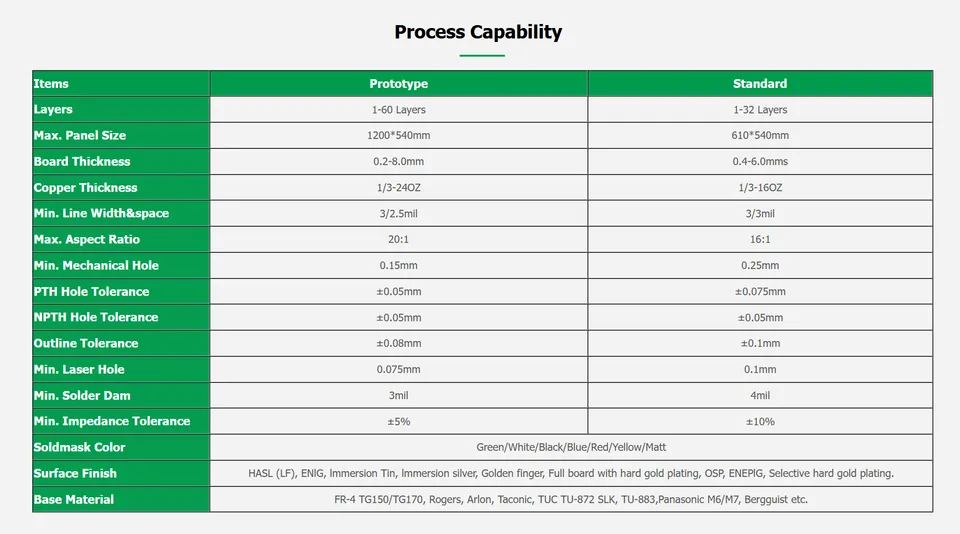
Specifica delle capacitàTabella capacità di processo PCB
Scarica documentoDai dati alla spedizione
Dai dati alla spedizione
Engineering review
Our PCB engineering team reviews Gerber or ODB++ data, stack-up requirements, drilling specifications, trace geometry and manufacturing tolerances. DFM analysis helps identify potential fabrication risks and confirm the production requirements before quotation and manufacturing.
Material & stackup
We evaluate PCB laminate materials, dielectric thickness, copper weight and layer configuration according to the application's electrical, thermal and mechanical requirements. Material and stack-up reviews support multilayer, HDI, high-speed, RF and rigid-flex PCB manufacturing.
Precision fabrication
Our PCB fabrication process integrates inner-layer imaging, etching, multilayer lamination, mechanical and laser drilling, copper plating, solder mask application and surface finishing. Process selection and manufacturing controls are adapted to the approved PCB design and technical specifications.
Inspection & delivery
PCB quality verification may include AOI, dimensional inspection, electrical testing and impedance verification according to project requirements. After final inspection, boards are packaged and prepared for shipment, with relevant production and quality records supporting traceability and customer review.
RFQ / DFM
Invia il requisito. Ricevi un piano di fornitura producibile.
Invia Gerber o ODB++, stackup, materiali, quantità, data richiesta e test per la verifica tecnica e il preventivo.
Revisione tecnicaMateriali e stack-upFabbricazione