
Manufacturing intelligence
PCB manufacturing capabilities
A transparent capability framework for multilayer, HDI, high-speed, RF and rigid-flex builds.
Get a factory-direct quoteJETFGO / PCB manufacturing capabilities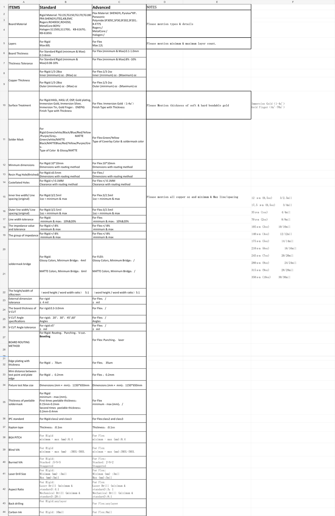 PRODUCT & PROCESS DETAIL
PRODUCT & PROCESS DETAILTECHNICAL WINDOW
Confirm manufacturing fit before you quote your customer.
Use published process limits, equipment and inspection controls to qualify the order, explain constraints and prepare a more complete customer quotation.
EXTENDED PORTFOLIO
Confirm manufacturing fit before you quote your customer.
A transparent capability framework for multilayer, HDI, high-speed, RF and rigid-flex builds.
07
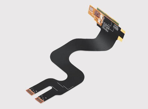
Flexible PCB Manufacturer
Fine-feature flex circuits with sheet or roll-to-roll production and assembly-test support.
View details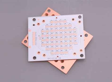
08
Metal Base PCB Manufacturer
Aluminum, copper and specialty metal-base constructions for demanding thermal and power designs.
View details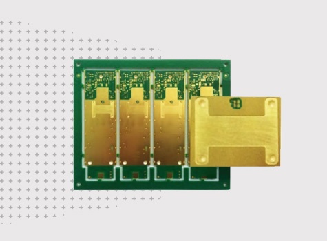
10
Copper Inlay PCB
Embedded copper inlays create a direct thermal path for high-power and high-heat-density assemblies.
View details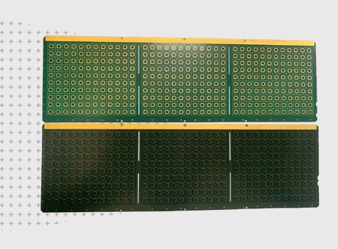
11
Substrate-Like PCB (SLP)
Fine-line, any-layer interconnect technology for compact high-density modules, subject to engineering review.
View details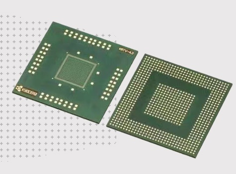
12
ABF IC Substrate
Ultra-fine ABF package substrate capability for advanced semiconductor interconnects, subject to engineering review.
View details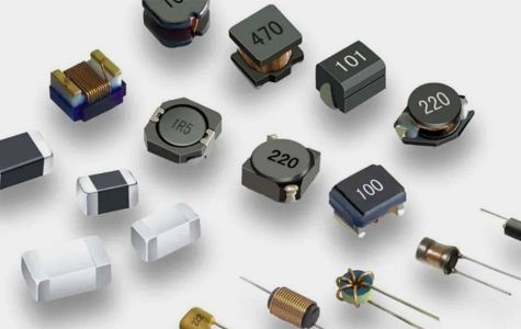
15
Electronic Component Sourcing
BOM-based component sourcing, traceability review and supply coordination connected to PCBA delivery.
View detailsPCB PROCESS CAPABILITY
Confirm your design requirements with confidence
Review rigid and flexible PCB materials, dimensions, tolerances and special processes to confirm the right manufacturing path for your project.
| # | Capability item | Rigid PCB | Flex PCB | Engineering notes |
|---|---|---|---|---|
| 01 | Board Material | TG135, TG150, TG170, TG180 FR4: SHENGYI, ITEQ, KB, EMC Rogers: RO4003C, RO4350 Metal Core: BOYU Halogen-free: S1150G, S1170G, KB-6167G, KB-6165G | SHENGYI, Pyralux® KP, Panasonic Polyimide: SF305C, SF30, SF202, SF201, R-F775 | Please specify material types and construction details. |
| 02 | Layers | Maximum 60 layers | Maximum 12 layers | Please specify minimum and maximum layer count. |
| 03 | Board Thickness | 0.3–8.0 mm | 0.1–1.0 mm | — |
| 04 | Thickness Tolerance | 0.08–10% | 8–10% | — |
| 05 | Copper Thickness — Inner | 1/3–28 oz | 1/3–2 oz | Specify required finished copper weight. |
| 06 | Copper Thickness — Outer | 1/3–28 oz | 1/3–2 oz | Specify required finished copper weight. |
| 07 | Surface Treatment | HASL, lead-free HASL, OSP, gold plating, ENIG, immersion silver, immersion tin, gold finger, ENEPIG | ENIG: 1–4 μin | ENIG: 1–4 μin Gold finger: 4–70 μin Please specify soft/hard bondable gold thickness. |
| 08 | Solder Mask | Glossy: green, white, black, blue, red, yellow, purple, grey Matte: green, white, black, blue, red, yellow, purple, grey | Green or yellow coverlay / solder mask | Specify color and glossy or matte finish. |
| 09 | Minimum Dimensions | 10 × 10 mm | 10 × 10 mm | Specify dimensions and routing method. |
| 10 | Resin Plug Hole — Finished | ≤ 0.5 mm | — | Specify dimensions and routing method. |
| 11 | Castellated Holes | ±0.1 mm | ±0.1 mm | Specify clearance and routing method. |
| 12 | Inner Line Width / Spacing | Minimum 3 / 2.5 mil | Minimum 3 / 2.5 mil | 12 μm: 3 / 2.5 mil 17.5 μm: 3 / 4 mil 35 μm (1 oz): 4 / 4 mil 70 μm (2 oz): 8 / 8 mil 105 μm (3 oz): 10 / 10 mil 140 μm (4 oz): 12 / 12 mil 175 μm (5 oz): 14 / 14 mil 210 μm (6 oz): 16 / 16 mil 245 μm (7 oz): 20 / 20 mil 280 μm (8 oz): 24 / 24 mil 315 μm (9 oz): 28 / 28 mil 350 μm (10 oz): 30 / 30 mil |
| 13 | Outer Line Width / Spacing | Minimum 3 / 2.5 mil (1 oz) | Minimum 3 / 2.5 mil (1 oz) | — |
| 14 | Line Width Tolerance | 10–20% | 10–20% | — |
| 15 | Impedance Value & Tolerance | ±8% | ±8% | — |
| 16 | Group Impedance | ±8% | ±8% | — |
| 17 | Solder Mask Bridge | Glossy: minimum 4 mil Matte: minimum 6 mil | — | — |
| 18 | Silkscreen Height / Width | 5:1 ratio | 5:1 ratio | — |
| 19 | External Dimension Tolerance | ±4 mil | — | — |
| 20 | V-Cut Board Thickness | 0.3–3.0 mm | — | — |
| 21 | V-Cut Angle | 20°, 30°, 45°, 60° | — | — |
| 22 | V-Cut Angle Tolerance | ±5° | — | — |
| 23 | Board Routing | Routing, punching, V-cut, beveling | Punching, laser | — |
| 24 | Edge Plating Thickness | 70 μm | 35 μm | — |
| 25 | Test Point to Plate Edge | Minimum 0.2 mm | Minimum 0.2 mm | — |
| 26 | Fixture Test Maximum Size | 1150 × 650 mm | 1150 × 650 mm | — |
| 27 | Peelable Solder Mask Thickness | First coating: 0.15–0.2 mm Second coating: 0.2–0.4 mm | — | — |
| 28 | IPC Standard | Class 2 and Class 3 | Class 2 and Class 3 | — |
| 29 | Kapton Tape | 0.1 mm | 0.1 mm | — |
| 30 | BGA Pitch | 0.4 mm | 0.4 mm | — |
| 31 | Blind Via | 3–5 mil | 3–5 mil | — |
| 32 | Buried Via | Stacked: 5+N+5 Staggered | Stacked: 2+N+2 Staggered | — |
| 33 | Laser Drill Size | 3–5 mil | 3–5 mil | — |
| 34 | Aspect Ratio | Laser: 4:1 Mechanical: 20:1 | Laser: 3:1 Mechanical: 8:1 | — |
| 35 | Back Drilling | Any-layer | Any-layer | — |
| 36 | Carbon Ink | 10 mil | 8 mil | — |
Capability specificationPCB Process Capability Chart
Download documentFrom data package to shipment
From data package to shipment
Engineering review
Buy directly from the manufacturer. Our own factory teams review DFM, plan production and inspect your boards, with equipment and process records available for supplier qualification.
Material & stackup
Buy directly from the manufacturer. Our own factory teams review DFM, plan production and inspect your boards, with equipment and process records available for supplier qualification.
Precision fabrication
Buy directly from the manufacturer. Our own factory teams review DFM, plan production and inspect your boards, with equipment and process records available for supplier qualification.
Inspection & delivery
Buy directly from the manufacturer. Our own factory teams review DFM, plan production and inspect your boards, with equipment and process records available for supplier qualification.
RFQ / DFM
Discuss your next order directly with our factory.
Send the Gerber or ODB++, stackup, material, quantity, target date and test requirements. Our team will review feasibility and return a technical quotation for the order you manage.
Engineering reviewMaterial & stackupPrecision fabrication