High Speed PCB Manufacturing CapabilitySignal Integrity and High-Speed PCB Solutions
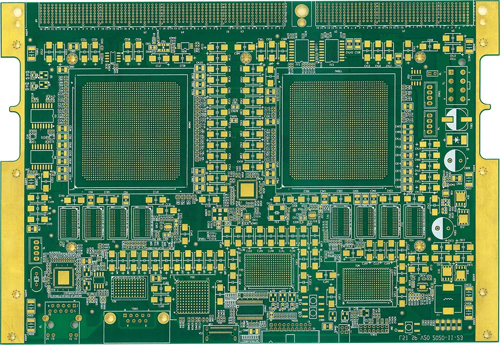
JETFGO is a Shenzhen-based high speed PCB manufacturer specializing in advanced PCB solutions for high-speed digital systems, computing platforms and communication equipment.
Our factory supports high speed PCB manufacturing with controlled impedance design, optimized stack-up structures, low-loss materials and reliable signal integrity control. From prototype validation to volume production, our engineering team helps customers achieve stable electrical performance for demanding electronic applications.
JETFGO high speed PCB solutions are widely used in AI servers, data communication systems, industrial computers, storage systems and other high-performance electronic products requiring fast signal transmission.
StackupControlled multilayer stack-up design · High-speed signal integrity optimization
ImpedanceSingle-ended impedance · Differential impedance · Controlled impedance testing
Testing & InspectionAOI inspection · Electrical testing · Impedance verification · Signal integrity control
MaterialsLow-loss FR-4 materials · High-speed laminates · Advanced PCB substrates
Layer CountMultilayer PCB capability for complex high-speed designs
Signal ApplicationHigh-speed digital signals · Data communication · Computing systems
Copper StructureOptimized copper thickness and routing structures for high-speed signal transmission
PCB TechnologyHDI · Multilayer PCB · High-speed PCB fabrication
High Speed PCB ApplicationsHigh-Speed Computing and Communication Applications
JETFGO high speed PCB solutions support electronic systems requiring fast signal transmission, power integrity control and reliable electrical performance.
High Speed PCB FAQCommon Questions About High Speed PCB Manufacturing
Learn about high speed PCB materials, impedance control, manufacturing capability, required files and production support.
08Common Questions About High Speed PCB Manufacturing
01What information is required for high speed PCB quotation?+
Customers can provide Gerber files or ODB++, stack-up information, layer count, material requirements, impedance specifications, quantity and surface finish requirements. Our engineering team will review the design before quotation.
02Can JETFGO manufacture prototype and production high speed PCB?+
Yes. JETFGO supports high speed PCB prototypes, NPI projects and volume production. Our engineering team provides support from stack-up review and material selection to final manufacturing.
03How is quality verified?+
High speed PCB quality is verified through AOI inspection, electrical testing, impedance verification, material control and production traceability to ensure stable signal performance.
04What is high speed PCB used for?+
High speed PCBs are used in applications requiring fast signal transmission, including AI servers, data communication equipment, computing systems, storage devices and advanced electronic products.
05How does JETFGO control signal integrity?+
JETFGO controls signal integrity through optimized stack-up design, controlled impedance, suitable material selection and electrical testing during PCB manufacturing.
06What materials are suitable for high speed PCB?+
High speed PCBs typically use low-loss FR-4 materials and advanced PCB substrates designed for stable electrical performance, signal integrity and high-speed transmission.
07Does JETFGO support controlled impedance PCB manufacturing?+
Yes. JETFGO supports controlled impedance PCB manufacturing with engineering review, stack-up optimization and electrical testing for high-speed digital and communication applications.
08Where is JETFGO high speed PCB factory located?+
JETFGO operates its PCB manufacturing facility in Shenzhen, China, providing high speed PCB fabrication and PCBA manufacturing support for global customers.

 PRODUCT & PROCESS DETAIL