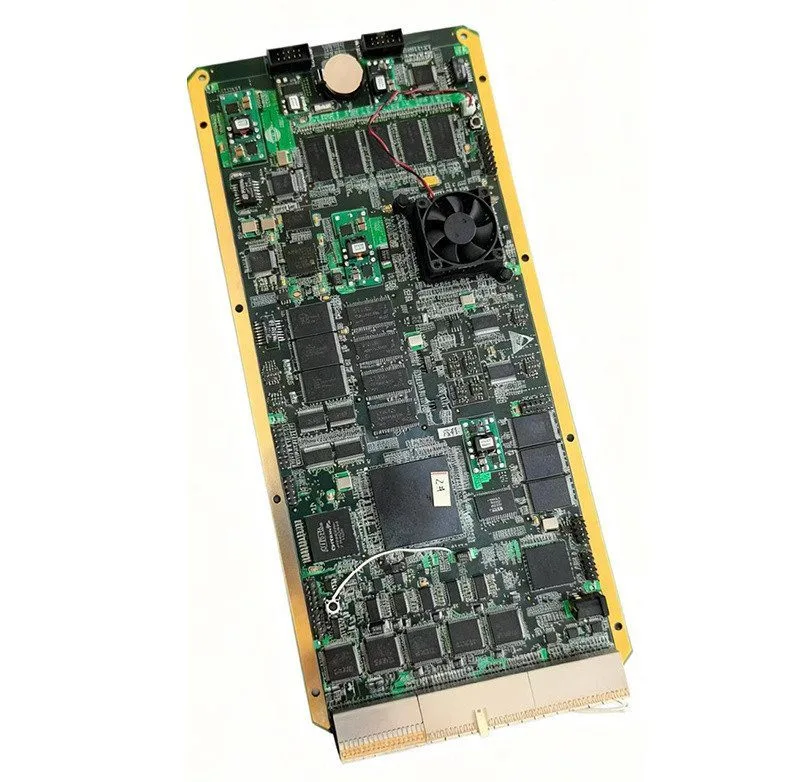
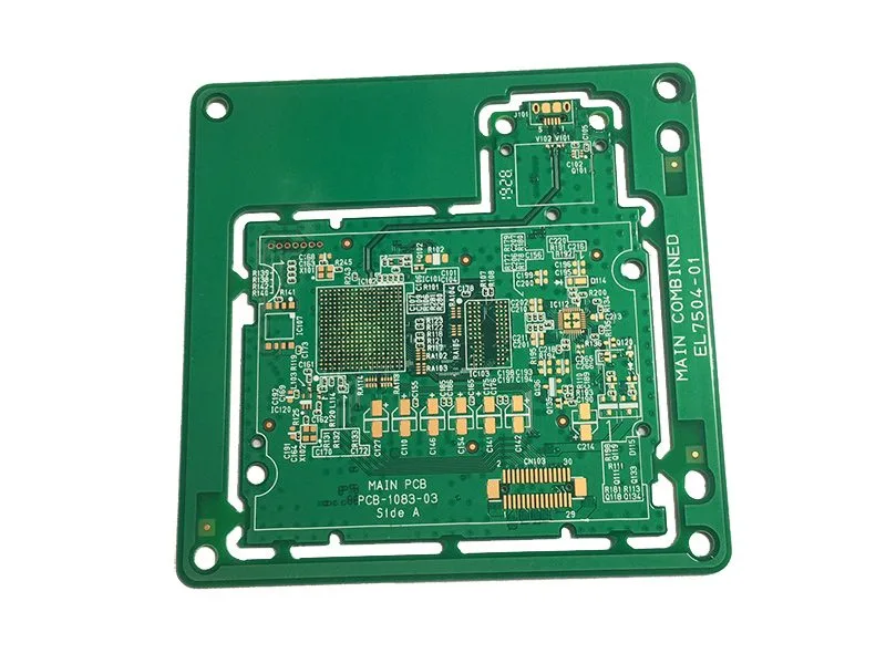
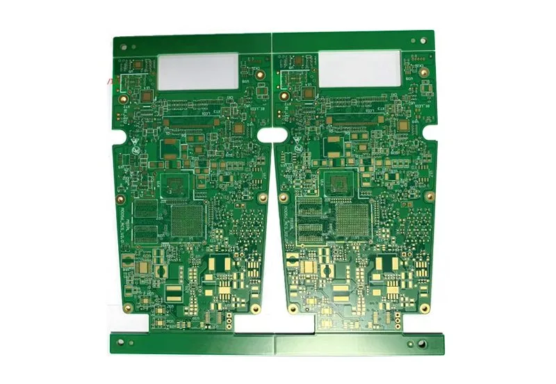
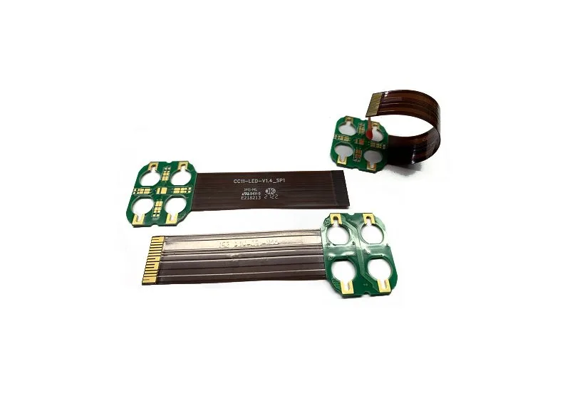
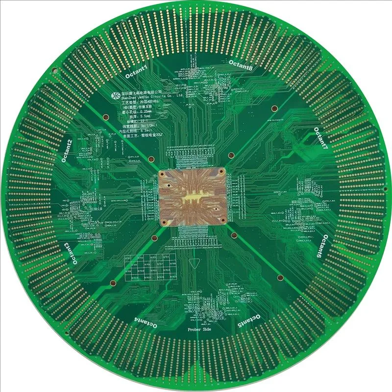
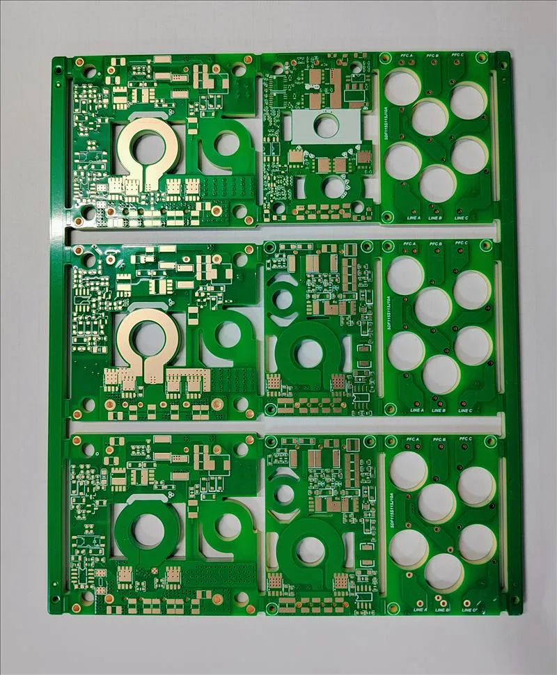
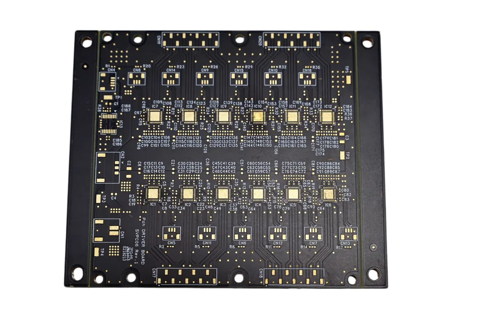
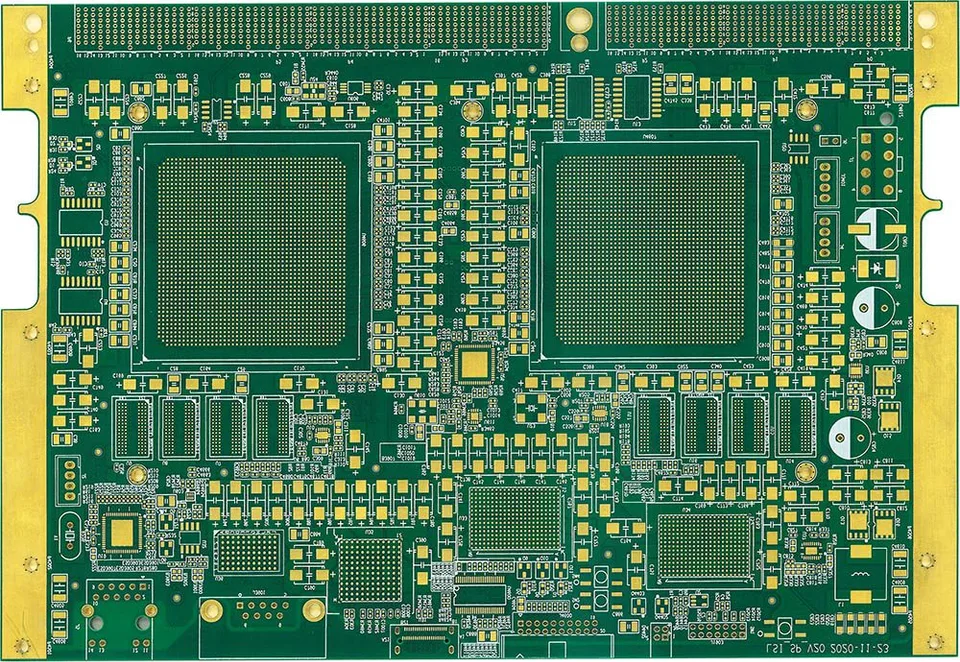
PCB ENGINEERING LIBRARY

PCB Knowledge Library & Manufacturing Resources

Explore JETFGO's PCB and PCBA knowledge library, featuring manufacturing processes, engineering insights, product examples, production equipment and quality control resources. Find practical information to support PCB design reviews, supplier evaluation and manufacturing decisions.

Get a factory-direct quote
JETFGO / PCB Knowledge Library & Manufacturing ResourcesPCB Knowledge Library & Manufacturing ResourcesPRODUCT & PROCESS DETAIL
SELECT A KNOWLEDGE PATH

Knowledge for better PCB decisions.

Explore JETFGO product examples, process capabilities, equipment, quality systems and manufacturing experience for your next project.

PCB ENGINEERING LIBRARY

PCB design & product guides

20
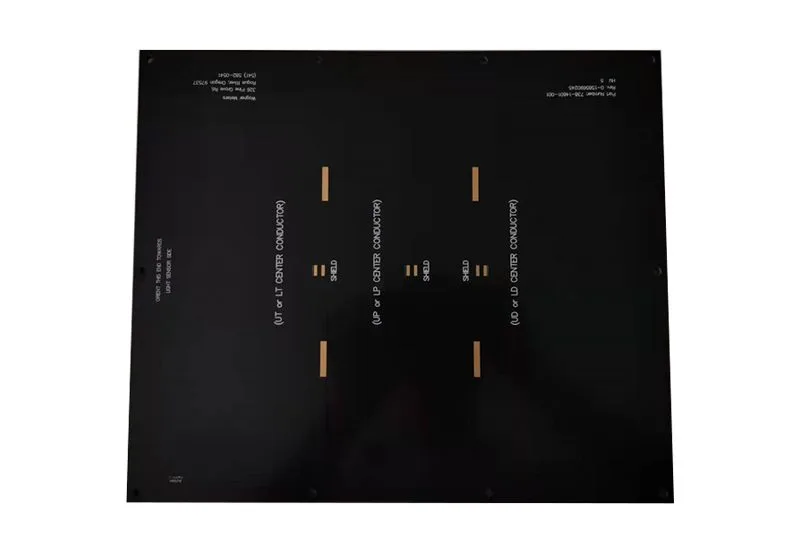
8.0 mm Thick 4-Layer PCB with Countersunk Holes
PCB design & product guides001

8.0 mm Thick 4-Layer PCB with Countersunk Holes

Explore JETFGO's 8.0 mm thick, 4-layer FR-4 PCB manufacturing example featuring VT-42 material, ENIG surface finish, precision countersunk holes and mechanical reinforcement. Discover key fabrication specifications and engineering considerations for extra-thick multilayer PCBs.

Full summary
Explore JETFGO's 8.0 mm thick, 4-layer FR-4 PCB manufacturing example featuring VT-42 material, ENIG surface finish, precision countersunk holes and mechanical reinforcement. Discover key fabrication specifications and engineering considerations for extra-thick multilayer PCBs.
View details
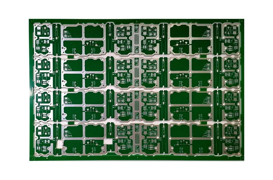
6-Layer Antenna PCB with Immersion Silver Finish
PCB design & product guides002

6-Layer Antenna PCB with Immersion Silver Finish

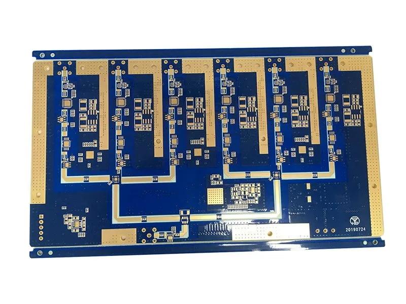
Explore JETFGO's 6-layer FR-4 antenna PCB manufacturing example featuring a 2.2 mm board thickness, immersion silver surface finish, 7.5/4 mil trace width and spacing, and controlled-impedance requirements for RF applications.

Full summary
Explore JETFGO's 6-layer FR-4 antenna PCB manufacturing example featuring a 2.2 mm board thickness, immersion silver surface finish, 7.5/4 mil trace width and spacing, and controlled-impedance requirements for RF applications.
View details
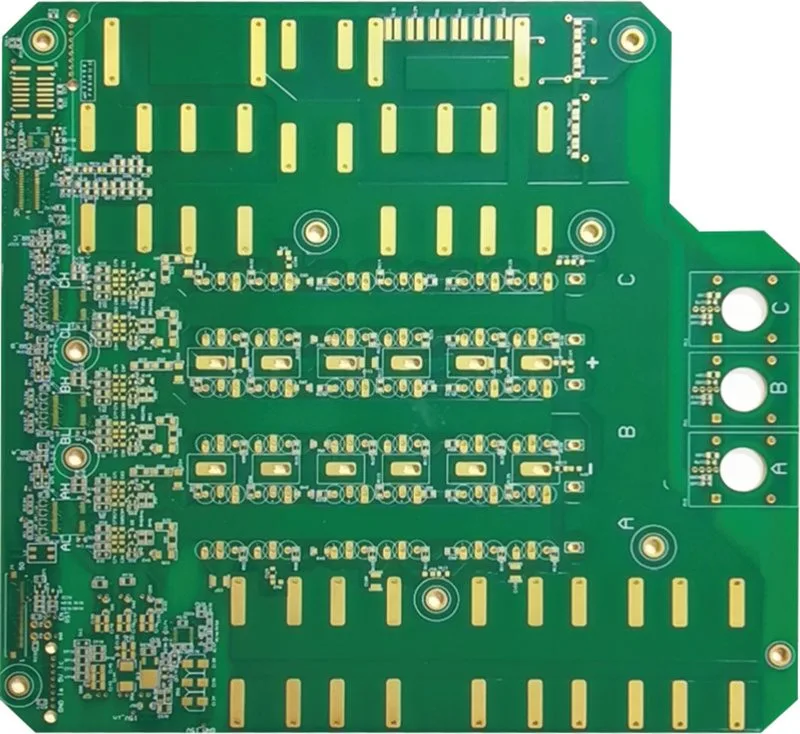
8-Layer Automotive PCB with Heavy Copper & Resin-Plugged Vias
PCB design & product guides003

8-Layer Automotive PCB with Heavy Copper & Resin-Plugged Vias

Explore JETFGO's 8-layer automotive PCB manufacturing example featuring Shengyi S1000-2M FR-4 material, 4.5 mm board thickness, ENIG surface finish, heavy-copper construction and resin plugging technology for automotive electronic applications.

Full summary
Explore JETFGO's 8-layer automotive PCB manufacturing example featuring Shengyi S1000-2M FR-4 material, 4.5 mm board thickness, ENIG surface finish, heavy-copper construction and resin plugging technology for automotive electronic applications.
View details
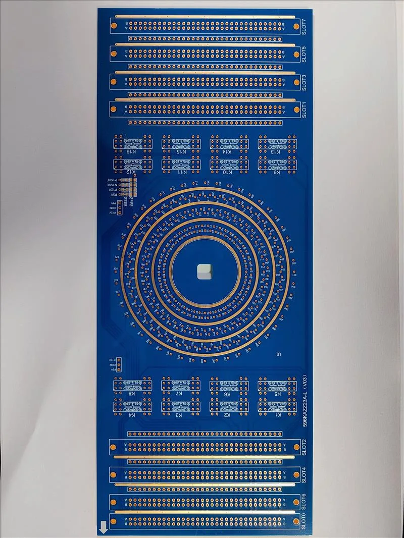
16-Layer Communication PCB with ENIG Surface Finish
PCB design & product guides004

16-Layer Communication PCB with ENIG Surface Finish

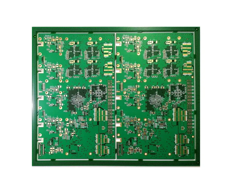
Explore JETFGO's 16-layer communication PCB manufacturing example featuring FR-4 S100-2M material, 4.0 mm board thickness, ENIG surface finish, 10/10 mil trace geometry and low-resistance design requirements for communication electronics.

Full summary
Explore JETFGO's 16-layer communication PCB manufacturing example featuring FR-4 S100-2M material, 4.0 mm board thickness, ENIG surface finish, 10/10 mil trace geometry and low-resistance design requirements for communication electronics.
View details
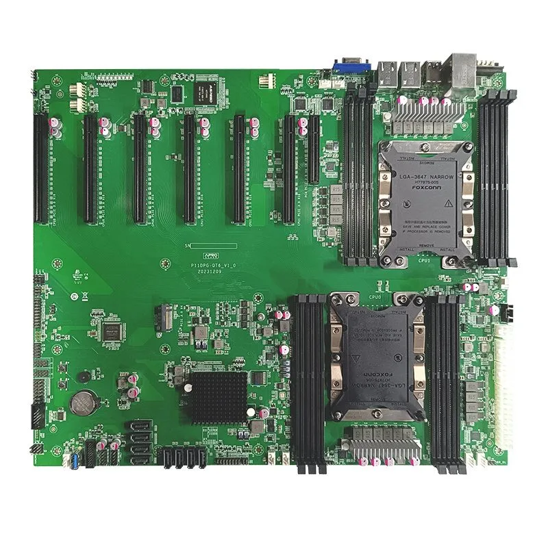
Computer PCB Manufacturing & Circuit Board Solutions
PCB design & product guides005

Computer PCB Manufacturing & Circuit Board Solutions

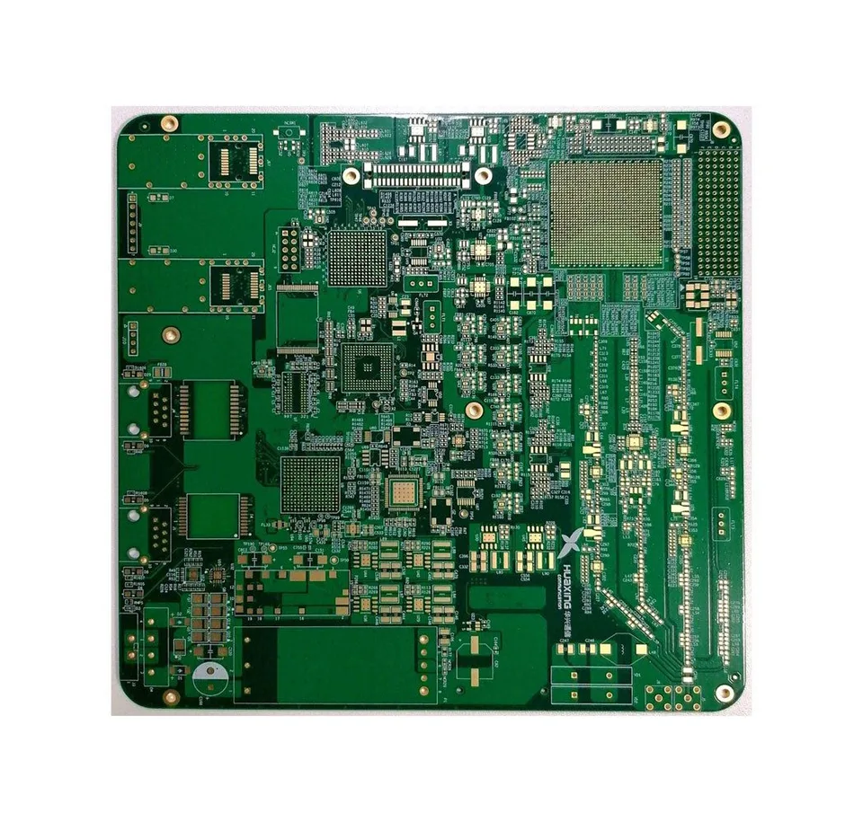
Explore JETFGO's PCB manufacturing solutions for computers, embedded computing systems and electronic control boards. Learn about multilayer PCB fabrication, material selection, manufacturing quality and PCBA assembly support for computing electronics.

Full summary
Explore JETFGO's PCB manufacturing solutions for computers, embedded computing systems and electronic control boards. Learn about multilayer PCB fabrication, material selection, manufacturing quality and PCBA assembly support for computing electronics.
View details
6-Layer Consumer Electronics PCB with OSP Finish
PCB design & product guides006

6-Layer Consumer Electronics PCB with OSP Finish

Explore JETFGO's 6-layer consumer electronics PCB featuring FR-4 material, 1.0 mm board thickness, OSP surface finish, 0.25 mm minimum holes and 3.5/3.5 mil fine-line routing for compact electronic applications.

Full summary
Explore JETFGO's 6-layer consumer electronics PCB featuring FR-4 material, 1.0 mm board thickness, OSP surface finish, 0.25 mm minimum holes and 3.5/3.5 mil fine-line routing for compact electronic applications.
View details
Conventional PCB Manufacturing & Application Examples
PCB design & product guides007

Conventional PCB Manufacturing & Application Examples

Explore JETFGO's conventional PCB manufacturing examples for industrial control, automotive electronics, communications, computers, medical devices, antennas and consumer electronics. Discover multilayer PCB fabrication capabilities and application-specific manufacturing solutions.

Full summary
Explore JETFGO's conventional PCB manufacturing examples for industrial control, automotive electronics, communications, computers, medical devices, antennas and consumer electronics. Discover multilayer PCB fabrication capabilities and application-specific manufacturing solutions.
View details
Rigid-Flex PCB Manufacturing & Applications
PCB design & product guides008

Rigid-Flex PCB Manufacturing & Applications

Explore JETFGO's rigid-flex PCB manufacturing capabilities, combining rigid circuit sections with flexible interconnections. Learn about multilayer construction, polyimide materials, bend requirements and manufacturing considerations for compact electronic assemblies.

Full summary
Explore JETFGO's rigid-flex PCB manufacturing capabilities, combining rigid circuit sections with flexible interconnections. Learn about multilayer construction, polyimide materials, bend requirements and manufacturing considerations for compact electronic assemblies.
View details
HDI PCB Manufacturing & High-Density Interconnect Technology
PCB design & product guides009

HDI PCB Manufacturing & High-Density Interconnect Technology

Explore JETFGO's HDI PCB manufacturing capabilities, including laser-drilled microvias, blind and buried vias, fine-line routing, sequential lamination and high-density BGA interconnections for advanced multilayer electronic applications.

Full summary
Explore JETFGO's HDI PCB manufacturing capabilities, including laser-drilled microvias, blind and buried vias, fine-line routing, sequential lamination and high-density BGA interconnections for advanced multilayer electronic applications.
View details
16-Layer Heavy Copper PCB with 4 oz Copper
PCB design & product guides010

16-Layer Heavy Copper PCB with 4 oz Copper

Explore JETFGO's 16-layer heavy copper PCB featuring 4 oz copper on inner and outer layers, FR-4 S1000-2M material, 3.6 mm board thickness and ENIG surface finish. Discover key manufacturing considerations for thick-copper multilayer circuit boards.

Full summary
Explore JETFGO's 16-layer heavy copper PCB featuring 4 oz copper on inner and outer layers, FR-4 S1000-2M material, 3.6 mm board thickness and ENIG surface finish. Discover key manufacturing considerations for thick-copper multilayer circuit boards.
View details
High Frequency Board
PCB design & product guides011

High Frequency Board

Explore JETFGO's high-frequency PCB manufacturing capabilities for RF, microwave and communication electronics. We support controlled-impedance PCB fabrication, Rogers high-frequency laminates and mixed-dielectric structures for demanding signal transmission applications.

Full summary
Explore JETFGO's high-frequency PCB manufacturing capabilities for RF, microwave and communication electronics. We support controlled-impedance PCB fabrication, Rogers high-frequency laminates and mixed-dielectric structures for demanding signal transmission applications.
View details
High-Speed PCB Manufacturing & Signal Integrity Solutions
PCB design & product guides012

High-Speed PCB Manufacturing & Signal Integrity Solutions

Explore JETFGO's high-speed PCB manufacturing capabilities, including multilayer stackup design, controlled impedance, low-loss dielectric materials and differential signal routing for data centers, AI computing, networking and high-speed communication electronics.

Full summary
Explore JETFGO's high-speed PCB manufacturing capabilities, including multilayer stackup design, controlled impedance, low-loss dielectric materials and differential signal routing for data centers, AI computing, networking and high-speed communication electronics.
View details
4-Layer Rogers 4350 + FR-4 Hybrid PCB
PCB design & product guides013

4-Layer Rogers 4350 + FR-4 Hybrid PCB

Explore JETFGO's 4-layer Rogers 4350 and FR-4 hybrid PCB featuring mixed-dielectric lamination, 1.2 mm board thickness, ENIG surface finish and 0.2 mm minimum holes. Discover hybrid PCB manufacturing for RF and high-frequency electronics.

Full summary
Explore JETFGO's 4-layer Rogers 4350 and FR-4 hybrid PCB featuring mixed-dielectric lamination, 1.2 mm board thickness, ENIG surface finish and 0.2 mm minimum holes. Discover hybrid PCB manufacturing for RF and high-frequency electronics.
View details
14-Layer Industrial PCB with Controlled Impedance
PCB design & product guides014

14-Layer Industrial PCB with Controlled Impedance

Explore JETFGO's 14-layer industrial PCB featuring FR-4 material, 2.0 mm board thickness, ENIG surface finish, 4.3/3.5 mil fine-line routing and controlled-impedance manufacturing for industrial electronic applications.

Full summary
Explore JETFGO's 14-layer industrial PCB featuring FR-4 material, 2.0 mm board thickness, ENIG surface finish, 4.3/3.5 mil fine-line routing and controlled-impedance manufacturing for industrial electronic applications.
View details
10-Layer Medical Electronics PCB with High-Tg FR-4
PCB design & product guides015

10-Layer Medical Electronics PCB with High-Tg FR-4

Explore JETFGO's 10-layer medical electronics PCB featuring High-Tg FR-4 material, 2.0 mm board thickness, ENIG surface finish, 5.4/3.5 mil fine-line routing and controlled-impedance manufacturing for medical electronic equipment.

Full summary
Explore JETFGO's 10-layer medical electronics PCB featuring High-Tg FR-4 material, 2.0 mm board thickness, ENIG surface finish, 5.4/3.5 mil fine-line routing and controlled-impedance manufacturing for medical electronic equipment.
View details
PCBA Manufacturing for Computing & Communication Boards
PCB design & product guides016

PCBA Manufacturing for Computing & Communication Boards

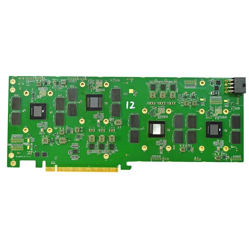
Explore JETFGO's PCBA manufacturing examples for privacy computing power boards, server boards, computer boards and communication modules. Our Shenzhen factory supports electronic component sourcing, SMT assembly, inspection and testing for prototype and repeat production.

Full summary
Explore JETFGO's PCBA manufacturing examples for privacy computing power boards, server boards, computer boards and communication modules. Our Shenzhen factory supports electronic component sourcing, SMT assembly, inspection and testing for prototype and repeat production.
View details
Privacy Computing Power Board | PCB & PCBA Manufacturing
PCB design & product guides017

Privacy Computing Power Board | PCB & PCBA Manufacturing

Explore JETFGO's PCB and PCBA manufacturing services for privacy computing power boards and specialized computing electronics. Our Shenzhen factory supports PCB fabrication, component sourcing, SMT assembly, inspection and manufacturing testing.

Full summary
Explore JETFGO's PCB and PCBA manufacturing services for privacy computing power boards and specialized computing electronics. Our Shenzhen factory supports PCB fabrication, component sourcing, SMT assembly, inspection and manufacturing testing.
View details
Server Board PCB & PCBA Manufacturing
PCB design & product guides018

Server Board PCB & PCBA Manufacturing

Explore JETFGO's PCB manufacturing and PCBA assembly services for server boards, data center electronics and computing hardware. Discover multilayer PCB fabrication, high-speed manufacturing, component sourcing, SMT assembly and quality inspection capabilities.

Full summary
Explore JETFGO's PCB manufacturing and PCBA assembly services for server boards, data center electronics and computing hardware. Discover multilayer PCB fabrication, high-speed manufacturing, component sourcing, SMT assembly and quality inspection capabilities.
View details
Special Technology PCB Manufacturing & Applications
PCB design & product guides019

Special Technology PCB Manufacturing & Applications

Explore JETFGO's special technology PCB manufacturing capabilities, including heavy-copper boards, thermal-electric separation PCBs, 8.0 mm extra-thick boards, extra-long PCBs and reinforced circuit boards. Discover advanced fabrication solutions for complex electronic applications.

Full summary
Explore JETFGO's special technology PCB manufacturing capabilities, including heavy-copper boards, thermal-electric separation PCBs, 8.0 mm extra-thick boards, extra-long PCBs and reinforced circuit boards. Discover advanced fabrication solutions for complex electronic applications.
View details
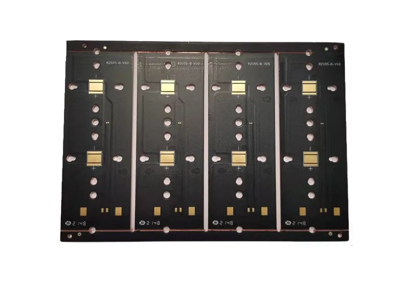
2-Layer Copper-Base PCB with Thermal-Electrical Separation
PCB design & product guides020

2-Layer Copper-Base PCB with Thermal-Electrical Separation

Explore JETFGO's 2-layer copper-base PCB featuring ST115B material, 3.2 mm board thickness, ENIG surface finish, 1.6 mm minimum holes and 8/8 mil trace geometry. Discover thermal-electrical separation technology for specialized thermal management applications.

Full summary
Explore JETFGO's 2-layer copper-base PCB featuring ST115B material, 3.2 mm board thickness, ENIG surface finish, 1.6 mm minimum holes and 8/8 mil trace geometry. Discover thermal-electrical separation technology for specialized thermal management applications.
View details
PCB ENGINEERING LIBRARY

Manufacturing, equipment & quality

07
PCB Manufacturing Equipment & Factory Facilities
Manufacturing, equipment & quality022

PCB Manufacturing Equipment & Factory Facilities

Explore JETFGO's PCB manufacturing equipment and factory facilities in Shenzhen, China, including laser direct imaging (LDI), multilayer lamination, drilling, copper plating, ENIG and hard gold finishing, precision routing, and wastewater treatment systems.

Full summary
Explore JETFGO's PCB manufacturing equipment and factory facilities in Shenzhen, China, including laser direct imaging (LDI), multilayer lamination, drilling, copper plating, ENIG and hard gold finishing, precision routing, and wastewater treatment systems.
View details
PCB Manufacturing Capabilities & Process Specifications
Manufacturing, equipment & quality023

PCB Manufacturing Capabilities & Process Specifications

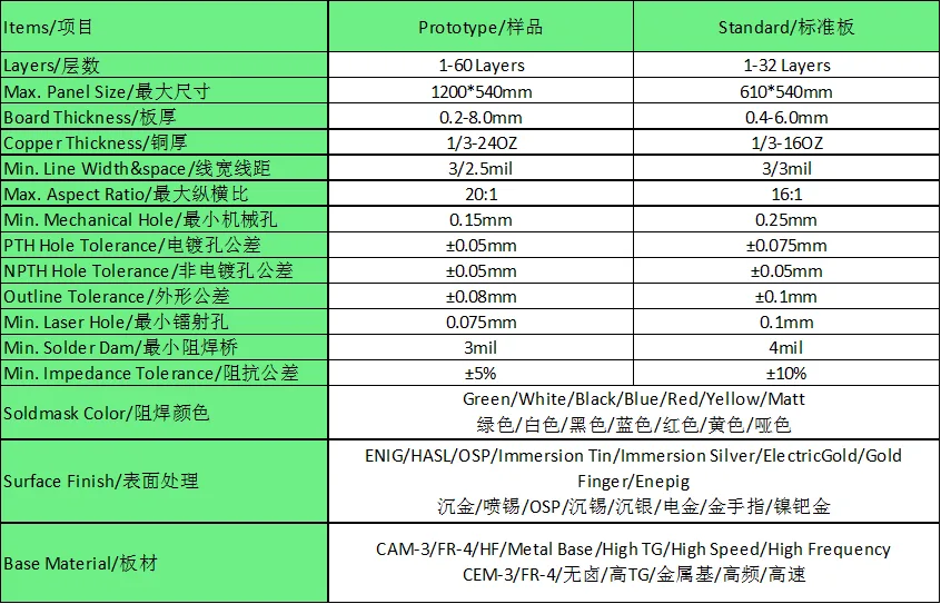
Explore JETFGO's PCB manufacturing capabilities, including multilayer fabrication, HDI microvias, fine-line processing, controlled impedance, rigid-flex circuits and advanced PCB materials. Discover key process considerations and engineering requirements for custom PCB production.

Full summary
Explore JETFGO's PCB manufacturing capabilities, including multilayer fabrication, HDI microvias, fine-line processing, controlled impedance, rigid-flex circuits and advanced PCB materials. Discover key process considerations and engineering requirements for custom PCB production.
View details
PCB Manufacturing Process Flow & Quality Control
Manufacturing, equipment & quality024

PCB Manufacturing Process Flow & Quality Control

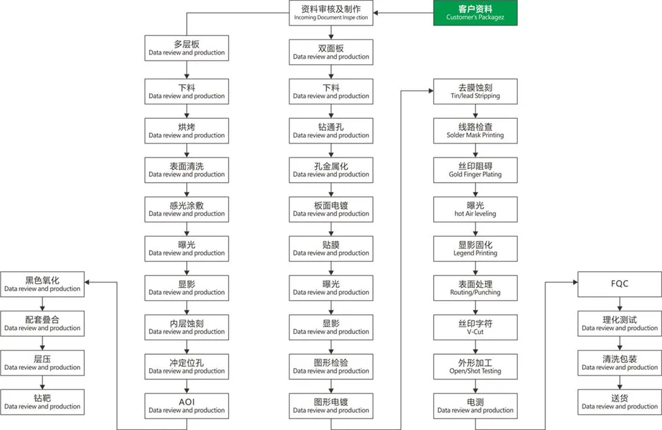
Explore JETFGO's PCB manufacturing process, from material inspection and inner-layer imaging to multilayer lamination, drilling, copper plating, etching, solder mask, surface finishing and electrical testing. Understand the key production stages and quality controls behind PCB fabrication.

Full summary
Explore JETFGO's PCB manufacturing process, from material inspection and inner-layer imaging to multilayer lamination, drilling, copper plating, etching, solder mask, surface finishing and electrical testing. Understand the key production stages and quality controls behind PCB fabrication.
View details
JETFGO 026
Manufacturing, equipment & quality026

Environmental Protection in PCB Manufacturing

Explore environmental management at JETFGO's PCB factory in Shenzhen, China. Learn about industrial wastewater treatment, chemical handling, manufacturing waste control and ISO 14001 environmental management practices in PCB production.

Full summary
Explore environmental management at JETFGO's PCB factory in Shenzhen, China. Learn about industrial wastewater treatment, chemical handling, manufacturing waste control and ISO 14001 environmental management practices in PCB production.
View details
JETFGO 027
Manufacturing, equipment & quality027

PCB Manufacturing Quality Control & Inspection

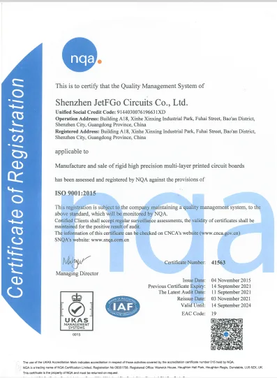
Explore JETFGO's PCB manufacturing quality control processes, including incoming material inspection, in-process quality checks, automated optical inspection (AOI), electrical testing and final inspection. Learn how our Shenzhen factory supports consistent PCB and PCBA manufacturing quality.

Full summary
Explore JETFGO's PCB manufacturing quality control processes, including incoming material inspection, in-process quality checks, automated optical inspection (AOI), electrical testing and final inspection. Learn how our Shenzhen factory supports consistent PCB and PCBA manufacturing quality.
View details
PCB ENGINEERING LIBRARY

Company & culture

03
JETFGO Company Culture, Mission & Core Values
Company & culture028

JETFGO Company Culture, Mission & Core Values

Discover JETFGO's company culture, vision, mission and core values. Since 2004, our Shenzhen PCB manufacturing business has emphasized innovation, integrity, teamwork, customer-focused service, manufacturing quality and continuous improvement.

Full summary
Discover JETFGO's company culture, vision, mission and core values. Since 2004, our Shenzhen PCB manufacturing business has emphasized innovation, integrity, teamwork, customer-focused service, manufacturing quality and continuous improvement.
View details
Company Profile
Company & culture029

Company Profile

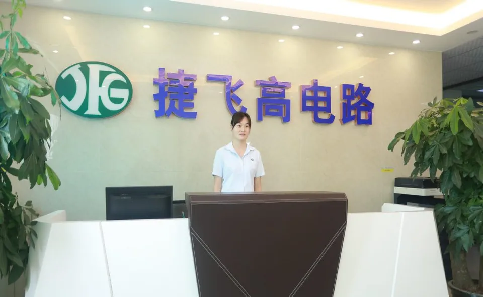
Shenzhen JETFGO Circuits Co Ltd. is a manufacturer whom specializing in the production of printed circuit boards in Shenzhen city. The company was established in 2004, and the factory is located in Fuhai Street, Bao'an D

Full summary
Shenzhen JETFGO Circuits Co Ltd. is a manufacturer whom specializing in the production of printed circuit boards in Shenzhen city. The company was established in 2004, and the factory is located in Fuhai Street, Bao'an D
View details
Shenzhen JETFGO Circuits Co.,Ltd.
Company & culture030

Shenzhen JETFGO Circuits Co.,Ltd.

Shenzhen JETFGO Circuits Co.,Ltd is a professional Printed Circuit Boards manufacturer in China. It was established in 1999, the factory was located at Fuyong Town, Bao’an District, Shenzhen.

Full summary
Shenzhen JETFGO Circuits Co.,Ltd is a professional Printed Circuit Boards manufacturer in China. It was established in 1999, the factory was located at Fuyong Town, Bao’an District, Shenzhen.
View details
ORIGINAL RECORDS

More from the JETFGO archive

Explore original company stories and event reports preserved from the earlier site.

RFQ / DFM

Discuss your next order directly with our factory.

Send the Gerber or ODB++, stackup, material, quantity, target date and test requirements. Our team will review feasibility and return a technical quotation for the order you manage.

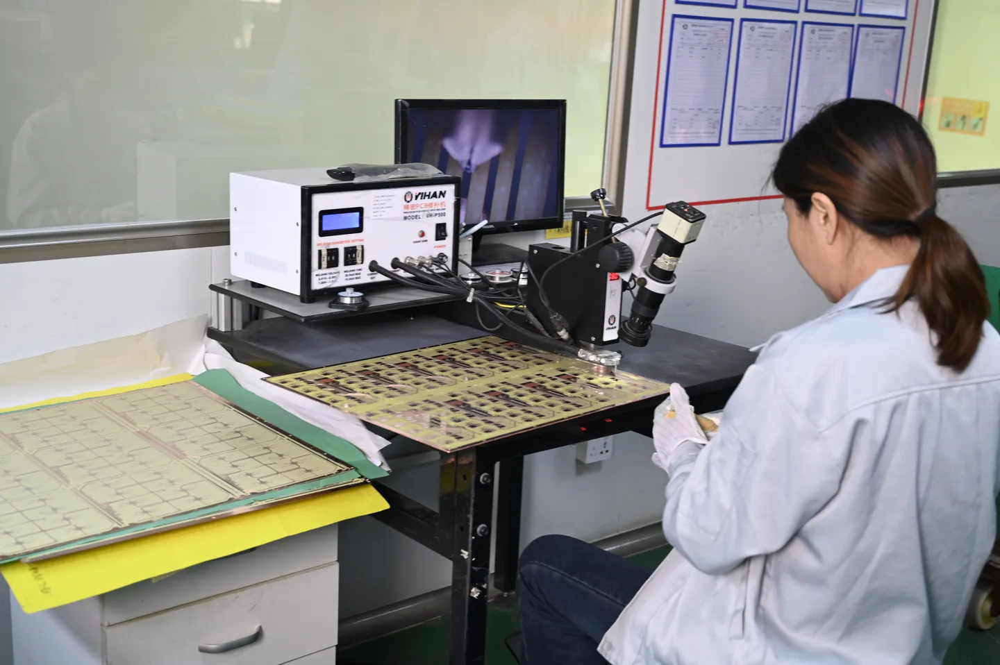
Engineering reviewMaterial & stackupPrecision fabrication