Back to engineering library
PCB design & product guides

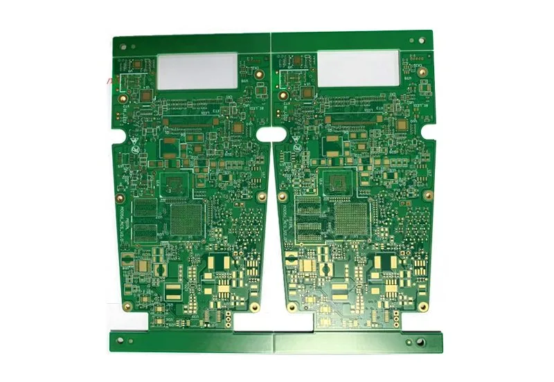
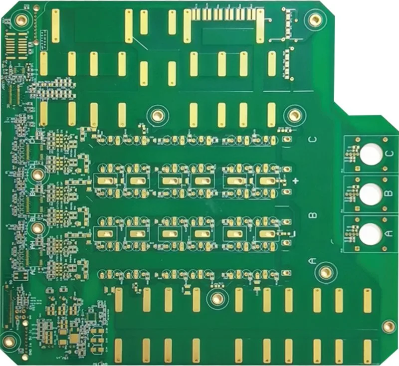
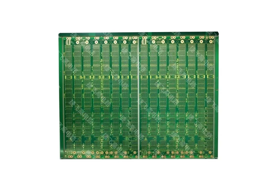
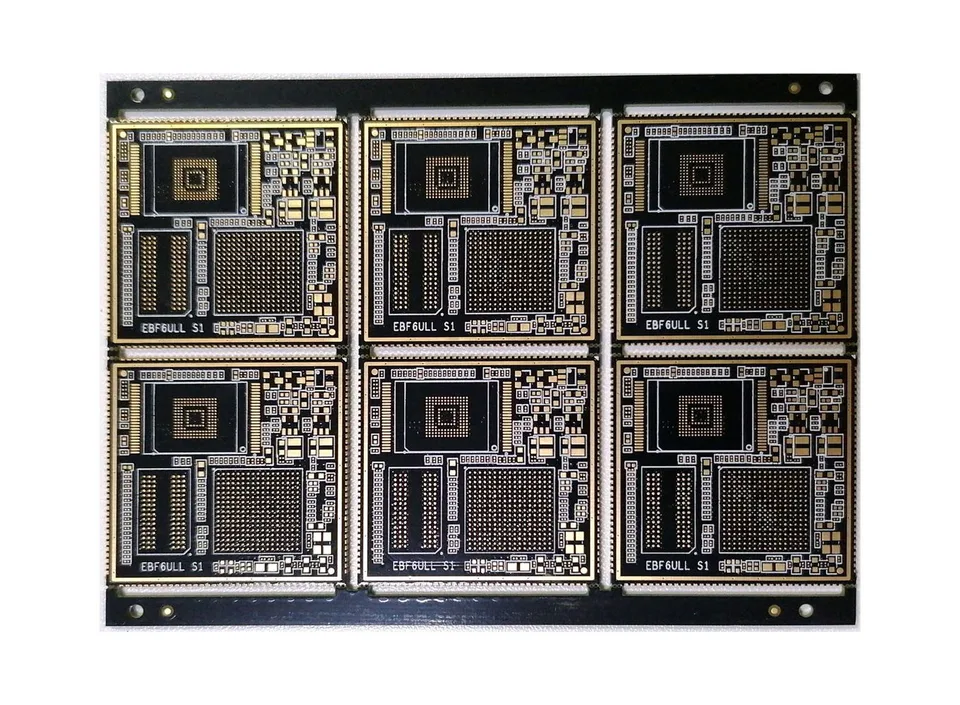
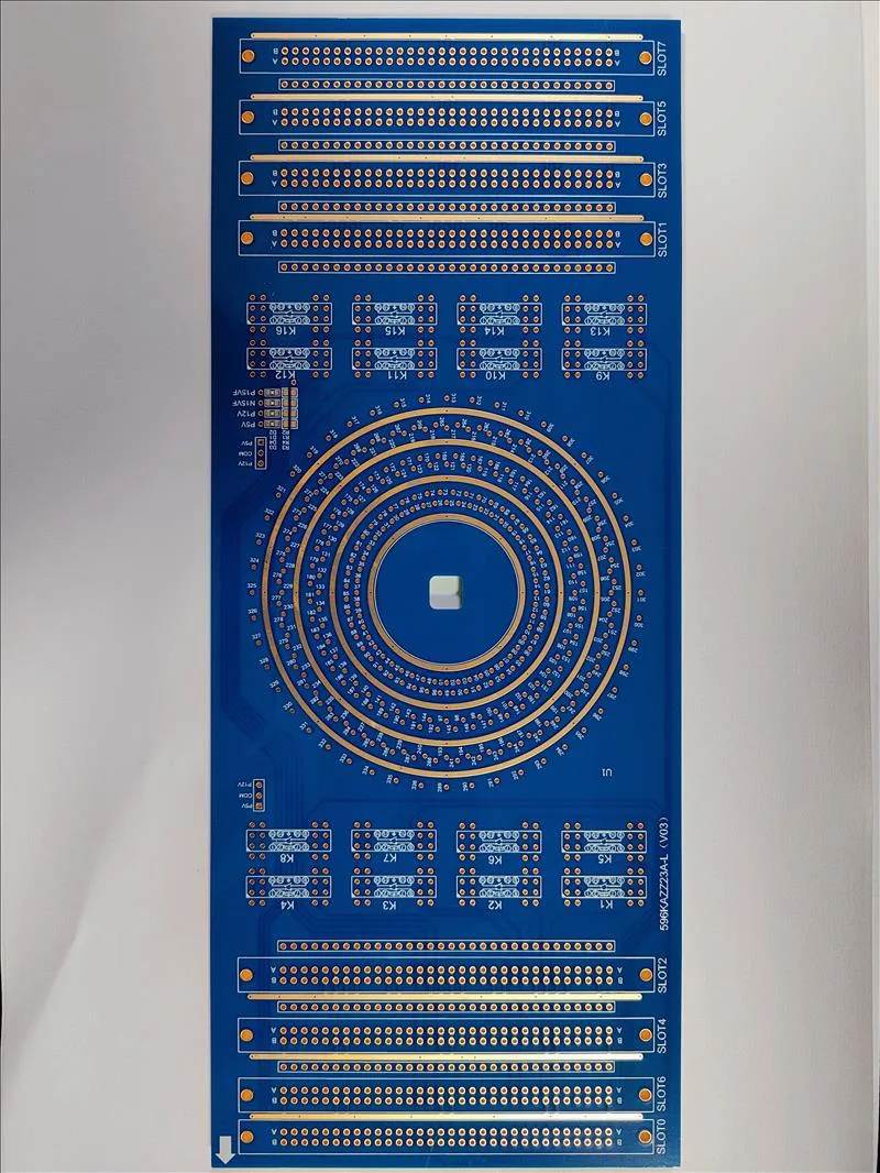
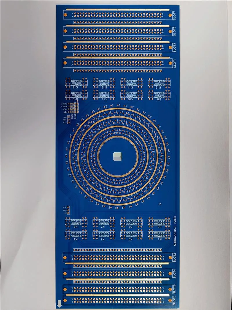
Communication Board

Layers: 16

Get a factory-direct quote
JETFGO / Communication BoardCommunication BoardPRODUCT & PROCESS DETAIL
PRODUCT / PROCESS DATA
Layers16
MaterialFR-4 S100-2M
Surface FinishENIG
Board Thickness4.0mm
Minimum Hole0.45mm
Line Width & Space10 / 10mil
Special TechnologyLower Resistance
E-mailsal@jetfgo.com
Tel0755-23300780 / 23302390
Fax0755-23302910
AddBuilding 18, District 1, Xinhe Xinxing Industrial Park, Fuhai Street, Baoan District, Shenzhen

Layers: 16
RFQ / DFM

Discuss your next order directly with our factory.

Send the Gerber or ODB++, stackup, material, quantity, target date and test requirements. Our team will review feasibility and return a technical quotation for the order you manage.

Engineering reviewMaterial & stackupPrecision fabrication
Contact Us