
Quick-turn PCB prototyping helps engineering teams verify a new design, test hardware and prepare for NPI without waiting for a full production cycle. JETFGO supports rapid PCB prototype manufacturing from simple boards to complex multilayer structures, with engineering review available for rigid PCBs up to 60 layers depending on the design and process requirements. Before production, our engineering team reviews Gerber or ODB++, drill data, stack-up, materials, board thickness, copper requirements, surface finish, impedance requirements and other fabrication details that may affect manufacturability or lead time. Our published capability reference for this solution includes engineering review for rigid PCBs up to 60 layers, minimum line / space of 3 / 2.5 mil and inspection options including AOI, flying probe and electrical testing. Quick-turn lead time is not a fixed promise for every project. Actual turnaround depends on layer count, materials, HDI or special processes, surface finish, testing requirements, file completeness and current manufacturing capacity. For engineering review, send Gerber or ODB++, drill files, proposed stack-up, fabrication drawing, quantity and target delivery date. Controlled-impedance, HDI or other special requirements should also be identified before quotation. Once the prototype is approved, the confirmed manufacturing data can support NPI and repeat low-to-medium volume production under the approved process conditions.
Published limits are drawn from JETFGO’s current capability chart. Final feasibility depends on the complete data package and engineering review.Quick-Turn PCB Prototype
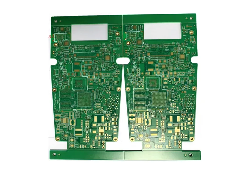
Quick-turn PCB prototyping for urgent design verification, engineering samples and NPI builds, with DFM review before production and a controlled path to repeat manufacturing.
Engineering answer
Verified process window
Quick-turn PCB prototyping for urgent design verification, engineering samples and NPI builds, with DFM review before production and a controlled path to repeat manufacturing.
Prototype Layer Capability
Engineering review up to 60-layer rigid PCB
Minimum Line / Space
3 / 2.5 mil
Inspection & Testing
AOI · flying probe · electrical test
Quick-Turn Lead Time
Confirmed after DFM, material availability and production-capacity review
Prototype Quantity
From 1 piece, subject to project review
Files for a useful review
Gerber or ODB++, drill files, proposed stack-up, fabrication drawing, quantity, target delivery date and any impedance, HDI or special-process requirements.
Provide final revision files, required quantity, board thickness, copper weight, surface finish, solder-mask requirements and target delivery date to reduce quotation and engineering clarification.
Technical questions
Published limits are drawn from JETFGO’s current capability chart. Final feasibility depends on the complete data package and engineering review.
01Does quick-turn PCB prototyping mean guaranteed 24-hour production?+
No. Quick-turn means the project is prioritized for rapid engineering review and manufacturing. Actual lead time depends on layer count, materials, board complexity, special processes, testing requirements, file completeness and current production capacity.
02Which files help JETFGO quote a quick-turn PCB prototype fastest?+
Send Gerber or ODB++, drill files, proposed stack-up, fabrication drawing, quantity and target delivery date. Include any impedance, HDI, special-material or testing requirements when applicable.
03Can JETFGO support prototype-to-production transfer?+
Yes. Once the prototype is validated, the approved manufacturing data, stack-up, materials and engineering record can support NPI and repeat low-to-medium volume production under the confirmed process conditions.
04What affects PCB prototype lead time?+
Lead time can be affected by layer count, materials, board thickness, HDI or controlled-impedance requirements, surface finish, special processes, testing requirements, file completeness and current production capacity.
05Does JETFGO have a minimum order quantity for PCB prototypes?+
No fixed MOQ is required for PCB prototyping. Prototype projects can start from 1 piece, subject to the board design, manufacturing process and engineering review.
06Can quick-turn PCB prototypes include controlled impedance or advanced multilayer structures?+
Yes. Controlled impedance, multilayer and other advanced PCB requirements can be reviewed for quick-turn prototyping, but the final manufacturing route and lead time depend on the complete design and process requirements.
Discuss your next order directly with our factory.
Send the Gerber or ODB++, stackup, material, quantity, target date and test requirements. Our team will review feasibility and return a technical quotation for the order you manage.