
SLP Engineering & DFM Review
Our engineers review fine-line routing, laser microvias, layer structure and manufacturing feasibility before production to identify risks early in the SLP project.
Substrate-like PCB (SLP) manufacturing with ultra-fine lines, laser microvias, any-layer interconnects and mSAP/amSAP processes for compact high-density electronics. JETFGO supports substrate-like PCB prototypes and production projects with in-house engineering and quality teams reviewing SLP stack-up, fine-line requirements, laser microvias and manufacturing feasibility before production.
Get a factory-direct quote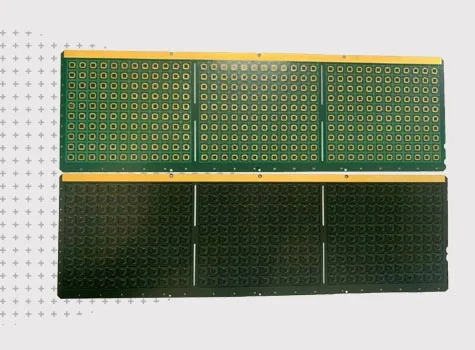 PRODUCT & PROCESS DETAIL
JETFGO is a Shenzhen-based substrate-like PCB (SLP) manufacturer providing ultra-fine-line and high-density interconnect solutions for advanced electronic products. Substrate-like PCB technology bridges the capability gap between conventional HDI PCB and IC substrate technology. By using advanced processes such as mSAP and amSAP, SLP structures can achieve finer line and space, smaller laser microvias and higher routing density than conventional PCB designs. JETFGO supports any-layer SLP structures up to 16 layers, laser microvias from 50 μm and fine line / space from 30 / 30 μm, subject to engineering review and project requirements. Our SLP manufacturing solutions are suitable for mobile devices, wearable electronics, advanced semiconductor-related systems, AI and high-performance computing modules, optical communication equipment, IoT devices and other compact electronics requiring high interconnect density. From engineering review and stack-up evaluation to fabrication, inspection and production support, JETFGO helps customers evaluate whether SLP, advanced HDI or another PCB technology is the most manufacturable solution for the project.
Work directly with our PCB manufacturing and engineering teams for SLP feasibility review, fine-line process evaluation, production control and inspection from prototype through scalable production.
Our engineers review fine-line routing, laser microvias, layer structure and manufacturing feasibility before production to identify risks early in the SLP project.
SLP stack-up structures are evaluated for routing density, microvia interconnection, material compatibility and manufacturing reliability.
mSAP and amSAP processes support ultra-fine circuit formation for high-density SLP designs beyond conventional subtractive PCB routing capability.
Production control focuses on fine-line integrity, laser microvia quality, layer registration, electrical testing and final inspection based on project requirements.
Laser microvias and any-layer interconnection provide routing flexibility for compact PCB structures requiring higher connection density.
JETFGO supports SLP projects from engineering evaluation and prototype validation through NPI and scalable production according to project requirements.
SLP technology supports electronic products requiring ultra-fine routing, high component density, compact form factors and advanced interconnection beyond conventional HDI PCB capability.
Find answers about SLP technology, mSAP manufacturing, fine-line capability, laser microvias, required files and application selection.
Please provide Gerber files or ODB++, fabrication drawings, stack-up, line and space requirements, microvia specifications, materials, quantity and surface finish requirements.
Yes. JETFGO supports substrate-like PCB engineering evaluation, prototype validation, NPI and scalable production based on design complexity and manufacturing requirements.
SLP quality verification may include fine-line inspection, laser microvia inspection, AOI, electrical testing, layer registration checks and final inspection based on project requirements.
A substrate-like PCB is an ultra-high-density PCB using finer circuit features and advanced processes such as mSAP to achieve routing density between conventional HDI PCB and IC substrate technology.
SLP generally uses finer line and space, smaller microvias and advanced additive or semi-additive processes compared with conventional HDI PCB, enabling higher routing density in compact electronics.
mSAP, or modified semi-additive process, forms fine copper circuits by selectively plating copper on a thin seed layer, enabling finer routing than conventional subtractive etching.
JETFGO supports SLP fine line and space from 30 / 30 μm, subject to stack-up, materials, design complexity and engineering review.
JETFGO supports laser microvias from 50 μm for applicable SLP and any-layer structures, subject to engineering review.
SLP is suitable for smartphones, wearable electronics, IoT devices, AR/VR products, AI and computing modules, optical communication equipment and other compact high-density electronics.
Send the Gerber or ODB++, stackup, material, quantity, target date and test requirements. Our team will review feasibility and return a technical quotation for the order you manage.