
A 1+N+1 HDI PCB uses one build-up layer on each side of an N-layer core, increasing routing density through laser-drilled microvias and sequential lamination. This construction is suitable for compact layouts, fine-pitch BGA fan-out and high-density electronic designs where conventional through-hole routing may consume too much board area. JETFGO reviews the complete HDI stack-up together with microvia geometry, dielectric thickness, capture pads, BGA escape routing, layer-to-layer interconnects and any via-in-pad requirements before confirming manufacturability. Our published capability reference for this solution includes 3–5 mil laser microvias and support for 0.4 mm BGA pitch. Final feasibility depends on the complete stack-up, BGA fan-out, pad geometry, copper structure, dielectric thickness and other project-specific requirements. Sequential lamination and laser drilling are key manufacturing processes for 1+N+1 HDI construction. Microvia placement, registration and any stacked, staggered or filled-via requirements should therefore be reviewed before production. For engineering review, provide Gerber or ODB++, drill files, proposed stack-up, fabrication drawing, quantity, target delivery date and applicable microvia, BGA or via-in-pad requirements. Published capability values are provided for initial selection. Final materials, HDI build-up, microvia structure and manufacturing feasibility are confirmed through project-specific engineering and DFM review.
Published limits are drawn from JETFGO’s current capability chart. Final feasibility depends on the complete data package and engineering review.1+N+1 HDI Microvia PCB
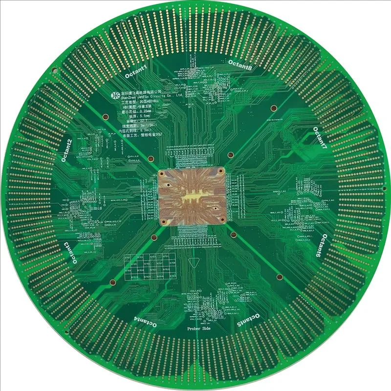
A 1+N+1 HDI PCB solution using laser-drilled microvias for compact layouts, high-density routing and fine-pitch BGA fan-out, subject to stack-up and DFM review.
Engineering answer
Verified process window
A 1+N+1 HDI PCB solution using laser-drilled microvias for compact layouts, high-density routing and fine-pitch BGA fan-out, subject to stack-up and DFM review.
HDI Build-Up
1+N+1 sequential lamination
Laser Microvia
3–5 mil
BGA Pitch
0.4 mm, subject to fan-out and DFM review
Microvia Structure
Laser-drilled blind microvia
HDI Process
Sequential lamination · laser drilling
Design Review
BGA fan-out · via-in-pad · microvia geometry · stack-up
Files for a useful review
Gerber or ODB++, drill files, proposed stack-up, fabrication drawing, quantity, target delivery date and applicable microvia, BGA or via-in-pad requirements.
Provide the proposed 1+N+1 layer structure, microvia layer pairs, dielectric thicknesses and any stacked, staggered or via-in-pad requirements.
Provide fine-pitch BGA locations, package pitch, pad geometry and any required via-in-pad or escape-routing constraints that may affect the HDI build-up.
Provide the preferred PCB thickness, copper weight, laminate or Tg requirements and any dielectric constraints relevant to the HDI stack-up.
Technical questions
Published limits are drawn from JETFGO’s current capability chart. Final feasibility depends on the complete data package and engineering review.
01Is 1+N+1 HDI suitable for every fine-pitch BGA design?+
No. 1+N+1 is a common HDI structure, but final suitability depends on BGA pitch, pad geometry, escape routing, microvia structure, stack-up and required routing density. More complex designs may require additional build-up layers.
02Which files help JETFGO review a 1+N+1 HDI PCB fastest?+
Send Gerber or ODB++, drill files, proposed stack-up, fabrication drawing, quantity, target delivery date and any microvia, BGA fan-out or via-in-pad requirements.
03Can JETFGO support prototypes and repeat production for 1+N+1 HDI PCBs?+
Yes. Once the HDI stack-up, microvia structure, materials and engineering requirements are confirmed, the approved manufacturing data can support prototype validation and repeat production under the same process conditions.
04What does 1+N+1 mean in an HDI PCB stack-up?+
1+N+1 describes an HDI construction with one build-up layer on each side of an N-layer core. Laser-drilled microvias connect the outer build-up layers to adjacent inner layers.
05What is a laser microvia in an HDI PCB?+
A laser microvia is a small laser-drilled interconnect used to connect adjacent PCB layers in an HDI structure. It enables higher routing density than conventional plated through-hole routing.
06Can JETFGO evaluate 0.4 mm BGA designs for 1+N+1 HDI?+
Yes. JETFGO can evaluate 0.4 mm BGA designs, but final feasibility depends on pad geometry, fan-out strategy, microvia size, via-in-pad requirements and the complete PCB stack-up.
07Does 1+N+1 HDI require sequential lamination?+
Yes. A 1+N+1 HDI structure uses build-up layers added around the core, so sequential lamination and laser-drilled microvias are part of the manufacturing process.
Discuss your next order directly with our factory.
Send the Gerber or ODB++, stackup, material, quantity, target date and test requirements. Our team will review feasibility and return a technical quotation for the order you manage.