
Dichteorientierter Aufbau für kompakte Layouts, Fine-Pitch-BGA und Laser-Microvias. Bestätigtes Prozessfenster: Blind via: 3–5 mil; Laser drill: 3–5 mil; BGA pitch: 0.4 mm Daten für die Prüfung: Gerber oder ODB++, Bohrdaten, Stack-up, Fertigungszeichnung, Menge und Zieltermin. Die veröffentlichten Grenzen stammen aus der aktuellen JETFGO-Fähigkeitsmatrix. Die endgültige Machbarkeit erfordert vollständige Daten.
Die veröffentlichten Grenzen stammen aus der aktuellen JETFGO-Fähigkeitsmatrix. Die endgültige Machbarkeit erfordert vollständige Daten.LösungscodeHDI-1N1Fähigkeit belegt
1+N+1 HDI-Microvia-PCB
Dichteorientierter Aufbau für kompakte Layouts, Fine-Pitch-BGA und Laser-Microvias.
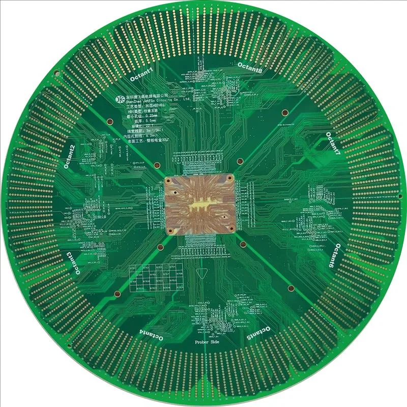
JETFGO / HDI-1N1RIGID
01 / TECHNISCHE ANTWORT
Technische Antwort
02 / DATA
Bestätigtes Prozessfenster
Dichteorientierter Aufbau für kompakte Layouts, Fine-Pitch-BGA und Laser-Microvias.
HDI Build-Up
1+N+1 sequential lamination
Laser Microvia
3–5 mil
BGA Pitch
0.4 mm, subject to fan-out and DFM review
Microvia Structure
Laser-drilled blind microvia
HDI Process
Sequential lamination · laser drilling
Design Review
BGA fan-out · via-in-pad · microvia geometry · stack-up
05 / INPUT
Daten für die Prüfung
HDI Engineering Review Package
Gerber or ODB++, drill files, proposed stack-up, fabrication drawing, quantity, target delivery date and applicable microvia, BGA or via-in-pad requirements.
HDI Stack-up & Via Structure
Provide the proposed 1+N+1 layer structure, microvia layer pairs, dielectric thicknesses and any stacked, staggered or via-in-pad requirements.
BGA Fan-Out Requirements
Provide fine-pitch BGA locations, package pitch, pad geometry and any required via-in-pad or escape-routing constraints that may affect the HDI build-up.
Material & Thickness Requirements
Angebot anfordernProvide the preferred PCB thickness, copper weight, laminate or Tg requirements and any dielectric constraints relevant to the HDI stack-up.
06 / FAQ
Technische Fragen
Die veröffentlichten Grenzen stammen aus der aktuellen JETFGO-Fähigkeitsmatrix. Die endgültige Machbarkeit erfordert vollständige Daten.
01Is 1+N+1 HDI suitable for every fine-pitch BGA design?+
No. 1+N+1 is a common HDI structure, but final suitability depends on BGA pitch, pad geometry, escape routing, microvia structure, stack-up and required routing density. More complex designs may require additional build-up layers.
02Which files help JETFGO review a 1+N+1 HDI PCB fastest?+
Send Gerber or ODB++, drill files, proposed stack-up, fabrication drawing, quantity, target delivery date and any microvia, BGA fan-out or via-in-pad requirements.
03Can JETFGO support prototypes and repeat production for 1+N+1 HDI PCBs?+
Yes. Once the HDI stack-up, microvia structure, materials and engineering requirements are confirmed, the approved manufacturing data can support prototype validation and repeat production under the same process conditions.
04What does 1+N+1 mean in an HDI PCB stack-up?+
1+N+1 describes an HDI construction with one build-up layer on each side of an N-layer core. Laser-drilled microvias connect the outer build-up layers to adjacent inner layers.
05What is a laser microvia in an HDI PCB?+
A laser microvia is a small laser-drilled interconnect used to connect adjacent PCB layers in an HDI structure. It enables higher routing density than conventional plated through-hole routing.
06Can JETFGO evaluate 0.4 mm BGA designs for 1+N+1 HDI?+
Yes. JETFGO can evaluate 0.4 mm BGA designs, but final feasibility depends on pad geometry, fan-out strategy, microvia size, via-in-pad requirements and the complete PCB stack-up.
07Does 1+N+1 HDI require sequential lamination?+
Yes. A 1+N+1 HDI structure uses build-up layers added around the core, so sequential lamination and laser-drilled microvias are part of the manufacturing process.
RFQ / DFM
Anforderung senden. Einen fertigbaren Lieferplan erhalten.
Senden Sie Gerber oder ODB++, Aufbau, Material, Menge, Zieltermin und Prüfanforderungen für Machbarkeitsprüfung und Angebot.
Engineering-PrüfungMaterial & Stack-upPräzisionsfertigung