
고밀도 레이아웃, 미세 피치 BGA 및 레이저 마이크로비아용. 검증된 공정 범위: Blind via: 3–5 mil; Laser drill: 3–5 mil; BGA pitch: 0.4 mm 검토용 파일: Gerber 또는 ODB++, 드릴 파일, 스택업, 제작 도면, 수량 및 목표 일정. 게시된 한계는 JETFGO의 현재 공정 능력표를 기반으로 하며 최종 가능성은 전체 자료 검토 후 확정됩니다.
게시된 한계는 JETFGO의 현재 공정 능력표를 기반으로 하며 최종 가능성은 전체 자료 검토 후 확정됩니다.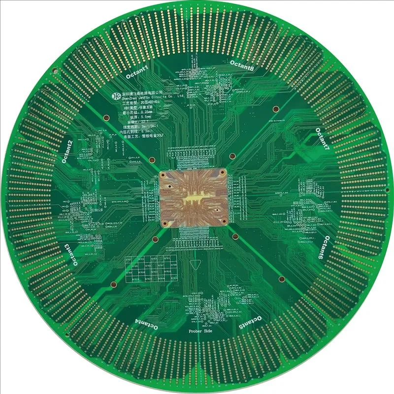
JETFGO / HDI-1N1RIGID
01 / 엔지니어링 답변
엔지니어링 답변
02 / DATA
검증된 공정 범위
고밀도 레이아웃, 미세 피치 BGA 및 레이저 마이크로비아용.
HDI Build-Up
1+N+1 sequential lamination
Laser Microvia
3–5 mil
BGA Pitch
0.4 mm, subject to fan-out and DFM review
Microvia Structure
Laser-drilled blind microvia
HDI Process
Sequential lamination · laser drilling
Design Review
BGA fan-out · via-in-pad · microvia geometry · stack-up
05 / INPUT
검토용 파일
HDI Engineering Review Package
Gerber or ODB++, drill files, proposed stack-up, fabrication drawing, quantity, target delivery date and applicable microvia, BGA or via-in-pad requirements.
HDI Stack-up & Via Structure
Provide the proposed 1+N+1 layer structure, microvia layer pairs, dielectric thicknesses and any stacked, staggered or via-in-pad requirements.
BGA Fan-Out Requirements
Provide fine-pitch BGA locations, package pitch, pad geometry and any required via-in-pad or escape-routing constraints that may affect the HDI build-up.
Material & Thickness Requirements
견적 요청Provide the preferred PCB thickness, copper weight, laminate or Tg requirements and any dielectric constraints relevant to the HDI stack-up.
06 / FAQ
기술 질문
게시된 한계는 JETFGO의 현재 공정 능력표를 기반으로 하며 최종 가능성은 전체 자료 검토 후 확정됩니다.
01Is 1+N+1 HDI suitable for every fine-pitch BGA design?+
No. 1+N+1 is a common HDI structure, but final suitability depends on BGA pitch, pad geometry, escape routing, microvia structure, stack-up and required routing density. More complex designs may require additional build-up layers.
02Which files help JETFGO review a 1+N+1 HDI PCB fastest?+
Send Gerber or ODB++, drill files, proposed stack-up, fabrication drawing, quantity, target delivery date and any microvia, BGA fan-out or via-in-pad requirements.
03Can JETFGO support prototypes and repeat production for 1+N+1 HDI PCBs?+
Yes. Once the HDI stack-up, microvia structure, materials and engineering requirements are confirmed, the approved manufacturing data can support prototype validation and repeat production under the same process conditions.
04What does 1+N+1 mean in an HDI PCB stack-up?+
1+N+1 describes an HDI construction with one build-up layer on each side of an N-layer core. Laser-drilled microvias connect the outer build-up layers to adjacent inner layers.
05What is a laser microvia in an HDI PCB?+
A laser microvia is a small laser-drilled interconnect used to connect adjacent PCB layers in an HDI structure. It enables higher routing density than conventional plated through-hole routing.
06Can JETFGO evaluate 0.4 mm BGA designs for 1+N+1 HDI?+
Yes. JETFGO can evaluate 0.4 mm BGA designs, but final feasibility depends on pad geometry, fan-out strategy, microvia size, via-in-pad requirements and the complete PCB stack-up.
07Does 1+N+1 HDI require sequential lamination?+
Yes. A 1+N+1 HDI structure uses build-up layers added around the core, so sequential lamination and laser-drilled microvias are part of the manufacturing process.
RFQ / DFM
요구사항을 보내고 실행 가능한 공급 계획을 받으세요.
Gerber 또는 ODB++, 적층, 재료, 수량, 목표 일정과 검사 요구를 보내주시면 기술 검토 후 견적합니다.
기술 검토소재·스택업정밀 제조