JETFGO / 고난도 PCB 프로젝트를 위한 정밀 제조.PRODUCT & PROCESS DETAIL
INSIDE OUR FACTORIES
Our PCB Factories. Our Manufacturing Processes.
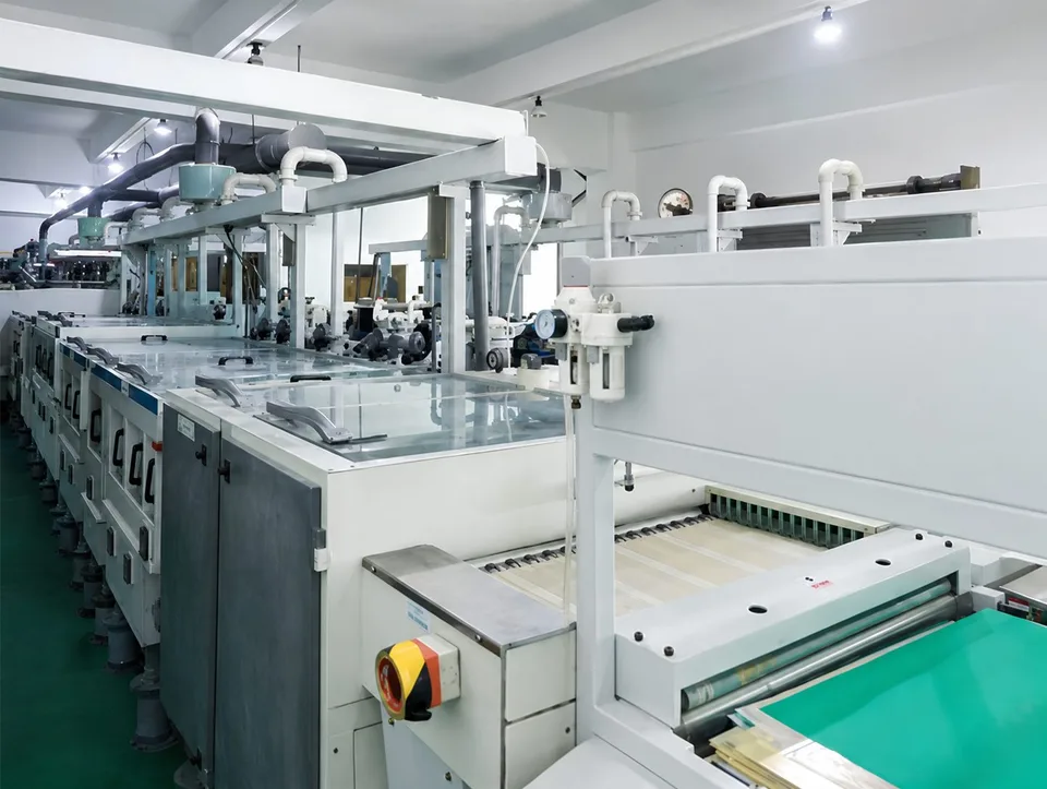
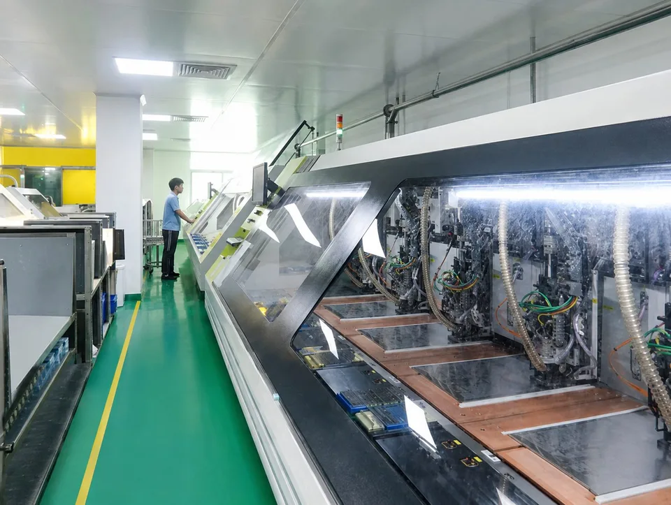
Take a closer look at how JETFGO manufactures printed circuit boards in Shenzhen. Explore our production equipment, engineering processes and inspection systems, and see the manufacturing capabilities behind the PCBs we deliver to customers worldwide.
01Established2004 · Shenzhen
02Monthly PCB capacity100,000 m²
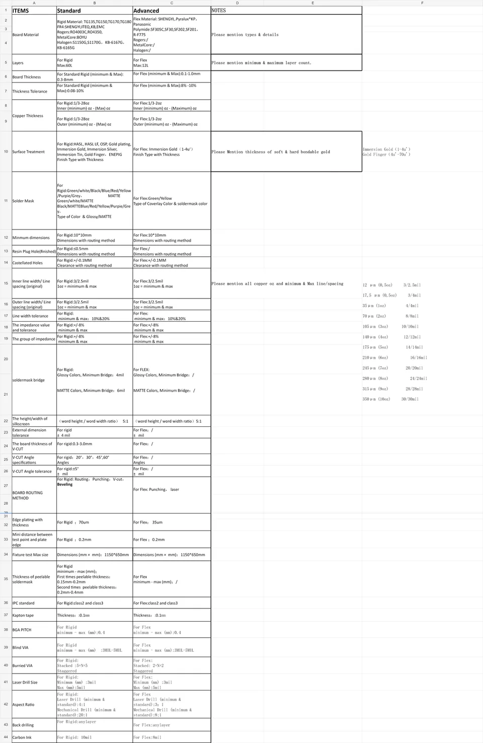
03Prototype capabilityUp to 60 layers
04Quality & complianceISO 9001 · IATF 16949 · UL
JETFGO / Shenzhen PCB Manufacturing사용 설비 · 관리 지점
자체 공장에서 기판이 완성되는 과정.
자체 공장에서 기판이 완성되는 과정.
각 단계의 설비, 관리 지점 및 자체 공장 사진을 확인하세요.
01
01 / 08
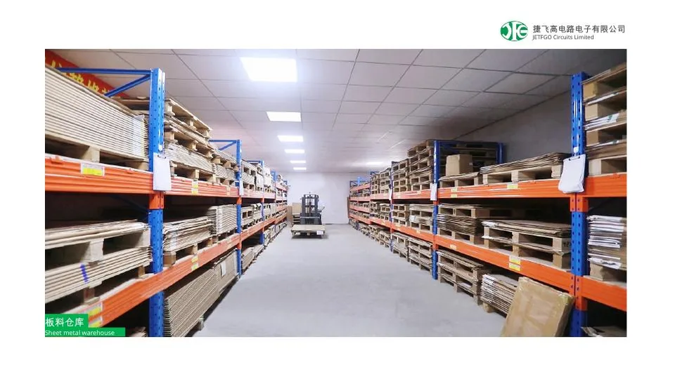
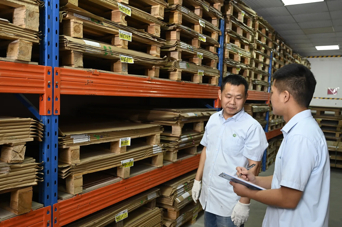
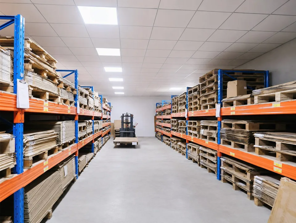
Incoming Material Inspection
Incoming laminates, copper foils and other PCB materials are checked against approved specifications. Manufacturing files and material requirements are reviewed before production begins.
사용 설비
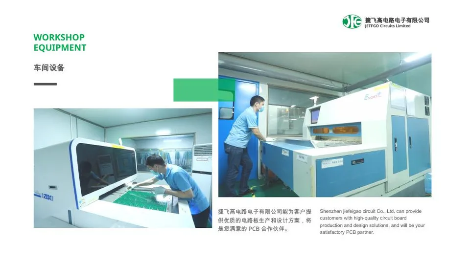
Material Inspection Equipment
관리 지점
Material identification, thickness verification, lot traceability and DFM approval.
02
02 / 08
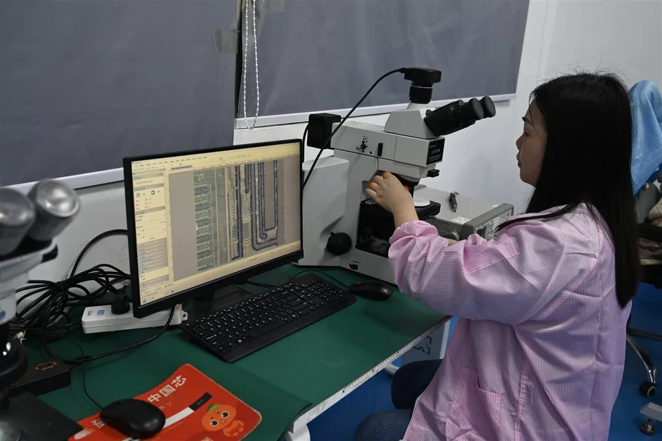
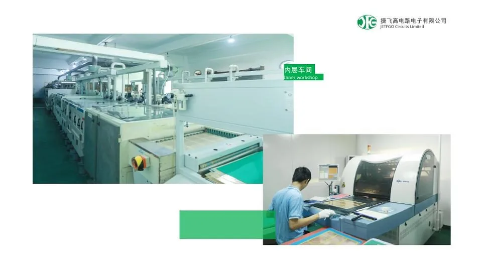
Inner-Layer Imaging & Etching
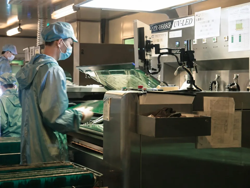
Circuit patterns are transferred onto copper-clad laminates through imaging and etching processes. Inner-layer AOI verifies circuit geometry before multilayer lamination.
사용 설비
Exposure System, Etching Line, AOI
관리 지점
Trace width, spacing, registration accuracy, open circuits and short circuits.
03
03 / 08
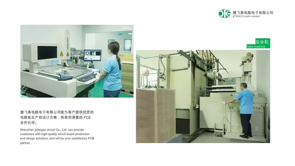
Multilayer PCB Lamination
Inner-layer cores and prepreg materials are stacked, aligned and bonded under controlled temperature and pressure to form a multilayer PCB structure.
사용 설비
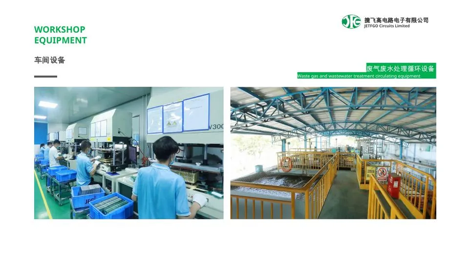
Multilayer Lamination Press
관리 지점
Layer alignment, finished thickness, bonding quality and delamination prevention.
04
04 / 08
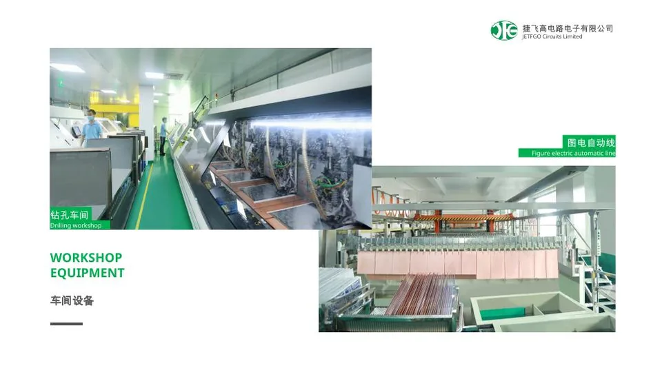
PCB Drilling & Hole Metallization
Mechanical drilling produces through-holes, while laser drilling supports suitable microvia structures. Desmear and through-hole metallization processes prepare the holes for reliable electrical interconnections.
사용 설비
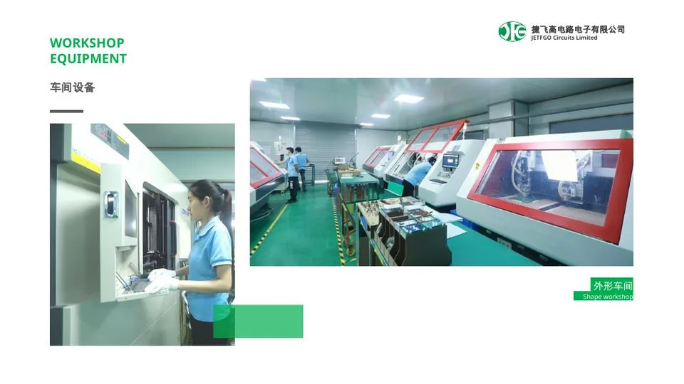
CNC Drilling Machines, Laser Drilling Equipment, PTH Line
관리 지점
Hole diameter, drilling registration, hole-wall quality and metallization integrity.
05
05 / 08
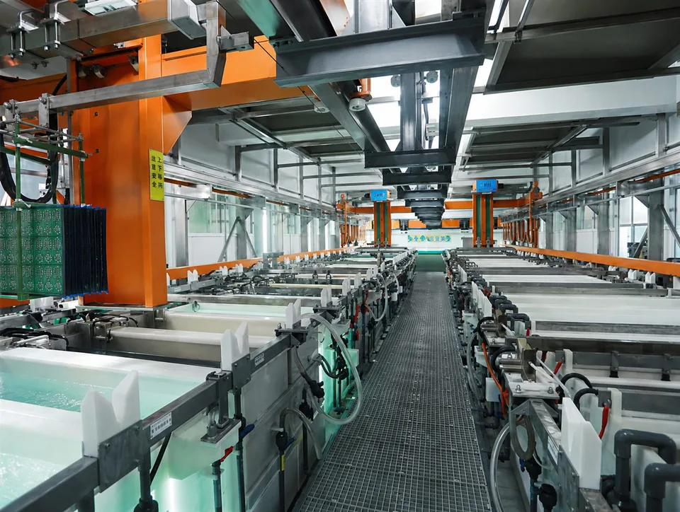
Outer-Layer Imaging, Plating & Etching
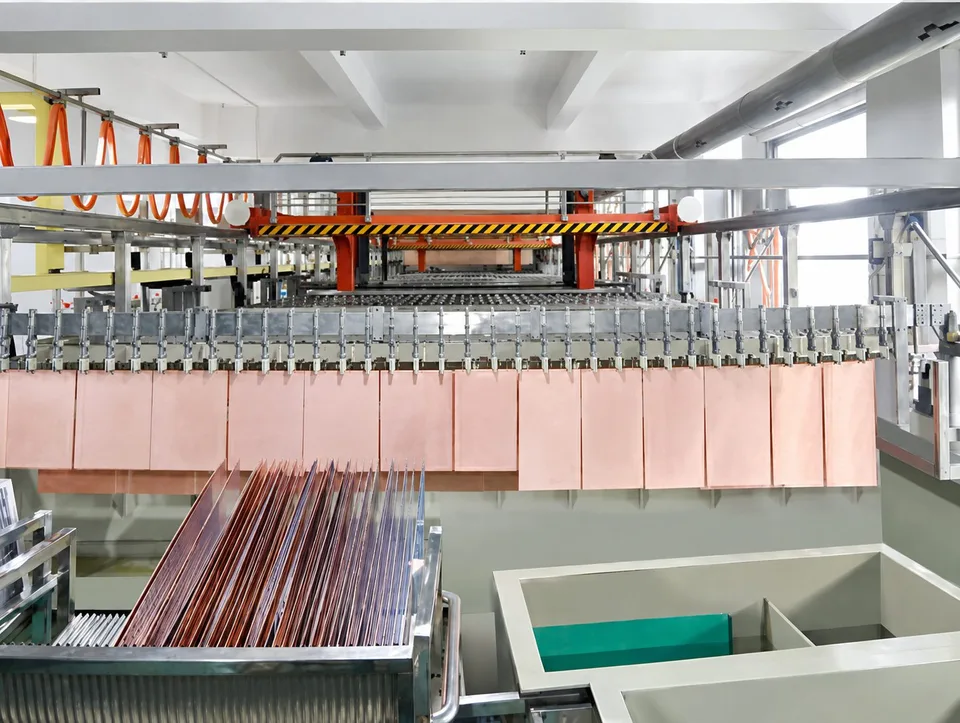
Outer-layer circuit patterns are formed through imaging, copper electroplating and selective etching. Process controls help maintain the specified conductor geometry and copper thickness.
사용 설비
Exposure System, Copper Plating Line, DES Line
관리 지점
Copper thickness, trace geometry, plating uniformity and circuit continuity.
06
06 / 08
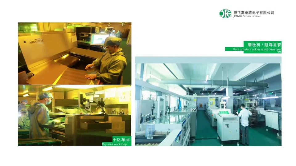
Solder Mask, Surface Finish & Profiling
Solder mask protects the circuitry, while legend printing provides component markings. The specified surface finish is applied, followed by precision routing to the required board outline.
Electrical continuity, open and short circuits, visual defects and final acceptance criteria.
08
08 / 08
Final Packaging & Shipment
Approved PCBs are counted, identified and packaged according to customer requirements. Final documentation and shipment checks are completed before dispatch.
사용 설비
Packaging Equipment, Labeling System
관리 지점
Order quantity, product identification, packaging protection, traceability and shipment approval.
자체 공장에서 기판이 완성되는 과정.
공장 역량
JETFGO의 공정 능력, 생산 설비, 검사 체계 및 제조 전문성을 확인하세요.
01 / JETFGO · 공장 역량02 / JETFGO · 공장 역량03 / JETFGO · 공장 역량04 / JETFGO · 공장 역량05 / JETFGO · 공장 역량06 / JETFGO · 공장 역량07 / JETFGO · 공장 역량08 / JETFGO · 공장 역량09 / JETFGO · 공장 역량
JETFGO / 공장 사진첩
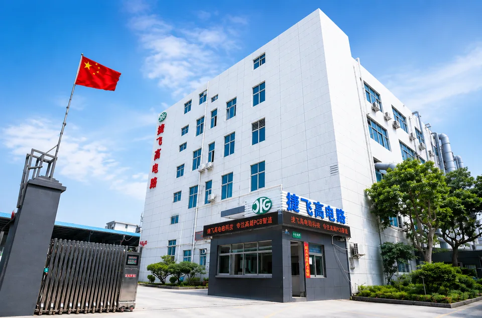
자체 공장 둘러보기
공장 부지, 생산 현장 및 설비의 실제 모습을 소개합니다.
사진을 준비 중입니다. 등록 후 공장 환경, 생산 현장 및 설비별로 표시됩니다.
생산 설비 · 검사 및 연구 장비
설비
생산 설비 · 검사 및 연구 장비
사용 설비
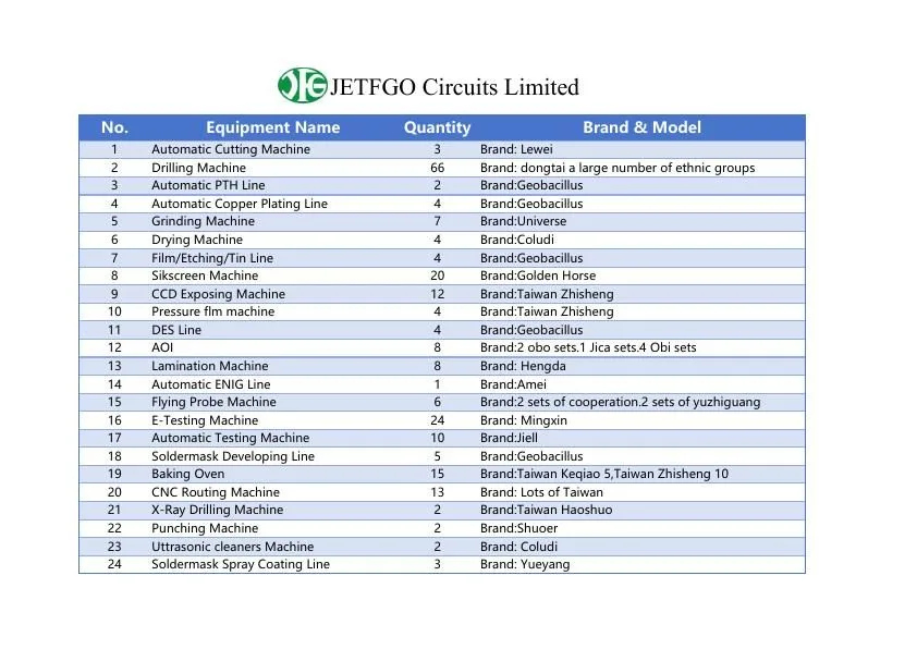
생산 설비
26
01Automatic cutting machine3
02Drilling machine66
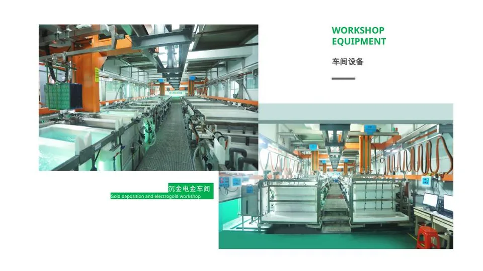
03Automatic PTH line2
04Automatic copper plating line4
05Grinding machine7
06Drying machine4
07Film / etching / tin line4
08Silkscreen machine20
09CCD exposing machine12
10Pressure film machine4
11DES line4
12AOI8
13Lamination machine8
14Automatic ENIG line1
15Flying probe machine6
16Electrical Testing Machine24
17Automatic Testing Machine10
18Soldermask developing line5
19Baking oven15
20CNC routing machine13
21X-Ray Target Drilling Machine2
22Punching machine2
23Ultrasonic cleaning machine2
24Soldermask spray coating line3
25Laser Direct Imaging (LDI) Machine5
26V-Cut Machine4
사용 설비
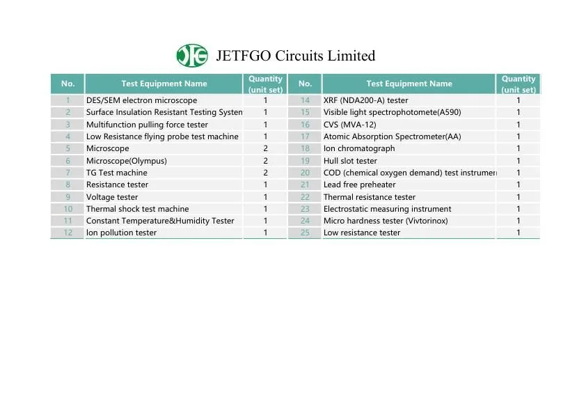
검사 및 연구 장비
26
01DES/SEM electron microscope1
02Surface insulation resistance system1
03Multifunction pulling force tester1
04Low-resistance flying probe tester1
05Microscope2
06Olympus microscope2
07TG test machine2
08Resistance tester1
09Voltage tester1
10Thermal shock test machine1
11Constant temperature & humidity tester1
12Ion contamination tester1
13XRF tester1
14Visible-light spectrophotometer1
15CVS analyzer1
16Atomic absorption spectrometer1
17Ion chromatograph1
18Hull cell tester1
19COD test instrument1
20Lead-free preheater1
21Thermal resistance tester1
22Electrostatic measuring instrument1
23Micro-hardness tester1
24Low-resistance tester1
25X-Ray Inspection System5
26Cross-Section Analysis System4
PCB ASSEMBLY EQUIPMENT
Equipment photographs and published parameters
Equipment names, photographs and parameters are sourced from the published JETFGO department page and remain editable in the admin portal.
01
ASSEMBLY / PRODUCTION
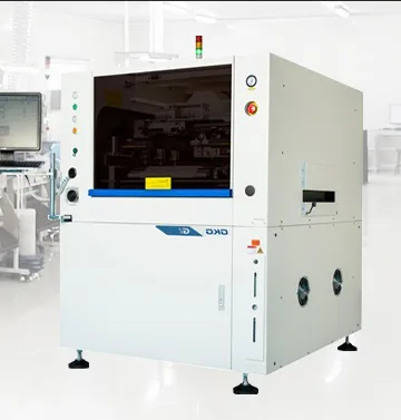
GKG Fully Automatic SMT Solder Paste Printer
The GKG fully automatic solder paste printer is used in JETFGO's SMT assembly lines to apply solder paste accurately onto PCB pads before component placement.
With automated PCB alignment and precision printing control, the equipment supports consistent solder paste deposition, reduces printing defects and improves assembly process stability for fine-pitch components and high-density PCBAs.
Maximum PCB Size
400 × 340 mm
System Alignment Accuracy & Repeatability
±0.01 mm
Solder Paste Printing Accuracy
±0.025 mm
02
ASSEMBLY / PRODUCTION
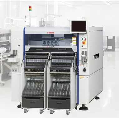
Yamaha YSM20 Automatic SMT Pick-and-Place Machine
The Yamaha YSM20 automatic SMT pick-and-place machine is used in JETFGO's PCBA production lines for precise placement of surface-mount electronic components onto printed circuit boards.
Supporting component sizes down to 01005 and a wide range of component types, the machine enables high-density PCB assembly, fine-pitch component placement and efficient SMT production.
Its automated placement system supports consistent component positioning, reduces assembly errors and improves manufacturing efficiency for prototype, small-batch and repeat PCBA production.
Supported PCB Size
50 × 50 mm – 400 × 340 mm
Placement Accuracy
0.025 mm
Minimum Component Size
01005
Maximum Supported Component Types
128
03
ASSEMBLY / PRODUCTION
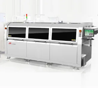
Automatic Wave Soldering Machine for PCBA Assembly
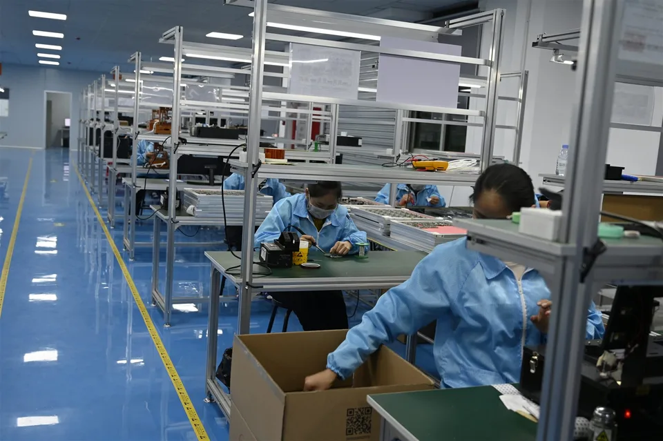
The automatic wave soldering machine is used in JETFGO's PCBA production lines for soldering through-hole (THT) electronic components onto printed circuit boards.
The process uses controlled flux application, preheating and molten solder contact to form electrical and mechanical connections between component leads and PCB pads.
With adjustable conveyor speed and controlled soldering conditions, the equipment supports consistent solder joint formation and efficient assembly of industrial control boards, power electronics and mixed-technology PCBAs.
Key quality considerations include solder joint coverage, hole filling, solder bridging and thermal exposure. Process settings are adjusted according to PCB construction, component requirements and the approved assembly specifications.
Preheating Time
Less than 15 minutes
Supported PCB Width
50–450 mm
PCB Conveyor Entry Height
750 ± 20 mm
Conveyor Speed Range
0–1800 mm/min
04
QUALITY / INSPECTION
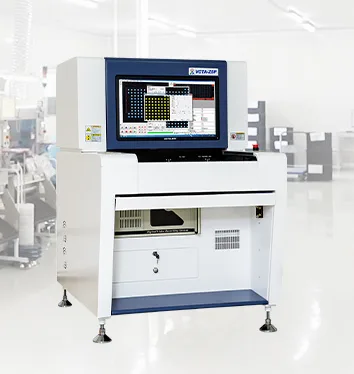
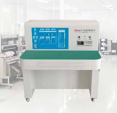
Automated Optical Inspection (AOI) System for PCBA
The Automated Optical Inspection (AOI) system is used in JETFGO's PCBA production lines to inspect component placement and visible solder-joint quality after SMT assembly.
Equipped with a 5-megapixel camera and 20 μm imaging resolution, the system supports automated identification of missing components, placement deviations, tombstoning, polarity errors, visible component damage and soldering defects.
AOI inspection helps detect potential manufacturing defects early, reduce manual inspection workload and improve consistency in PCB assembly quality.
The equipment supports quality control for prototype, small-batch and repeat PCBA production, with inspection criteria configured according to component types, PCB layouts and customer requirements.
SMT Intelligent First Article Inspection (FAI) System
The SMT Intelligent First Article Inspection (FAI) System is used in JETFGO's PCBA production lines to verify component parameters and assembly accuracy before batch production.
Equipped with a high-precision LCR measurement system, the equipment supports resistance, capacitance and inductance verification against approved component specifications.
First article inspection helps identify incorrect component values, material mismatches and potential assembly errors before mass production, reducing rework risks and improving manufacturing consistency.
This inspection process supports quality control during new product introduction (NPI), production changeovers and repeat PCBA manufacturing.
Measurement System
High-Precision LCR Bridge
Basic Measurement Accuracy
0.05%
Test Frequency Range
50 Hz – 100 kHz
Test Frequency Points
34
06
ASSEMBLY / PRODUCTION
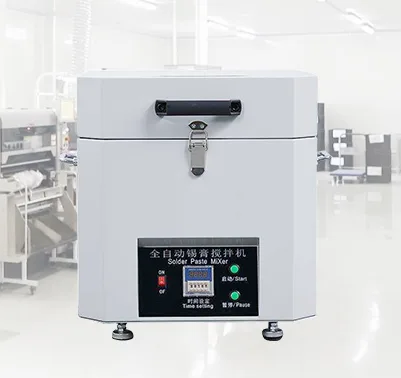
Fully Automatic SMT Solder Paste Mixer
The fully automatic solder paste mixer is used in JETFGO's SMT production lines to prepare solder paste before stencil printing and electronic component assembly.
The equipment provides controlled mixing to improve solder paste uniformity and consistency, helping maintain suitable printing conditions for accurate solder paste deposition on PCB pads.
With a dual-can mixing capacity and adjustable operating time, the system supports efficient solder paste preparation for prototype, small-batch and repeat PCBA production.
Consistent solder paste preparation helps reduce process variation and supports better solder paste printing quality. Mixing procedures are controlled according to solder paste specifications and production requirements.
Working Capacity
500 g × 2 Cans
Compatible Solder Paste Containers
M-Type Cans, Diameter Ø60–Ø67
Short-Duration Timer
0.1–99 s, 0.1 s Increments
Extended Timer
0.1–30 min, 0.1 min Increments
07
QUALITY / INSPECTION
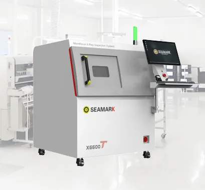
Microfocus X-Ray Inspection System for PCBA
The Microfocus X-Ray Inspection System is used in JETFGO's PCBA quality control process to examine internal solder joints and electronic assembly features that cannot be directly inspected through conventional optical inspection.
The equipment supports non-destructive inspection of hidden solder connections beneath BGA, QFN and other advanced semiconductor packages. X-ray imaging helps identify potential solder voids, bridging, insufficient solder and internal assembly defects.
Equipped with a sealed microfocus X-ray source, adjustable platform tilt and high-definition imaging, the system provides detailed views of complex solder joint structures.
X-ray inspection complements AOI and electrical testing, helping improve defect detection and manufacturing quality for high-density PCBAs, prototype validation and repeat production.
Inspection Stage Size
40 × 440 mm
Platform Tilt Angle
±30°
X-Ray Source Type
Sealed Reflection-Type Microfocus X-Ray Source
Field of View
65 × 65 mm
Image Resolution
1080p
Imaging Frame Rate
30 fps
Field-of-View Angle
90°
Digital Zoom
4×
08
QUALITY / INSPECTION
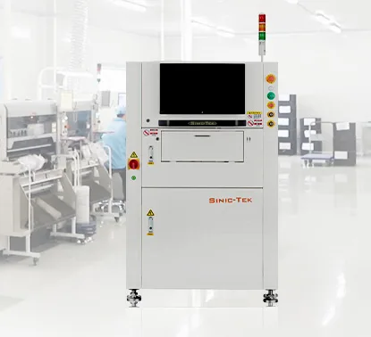
3D Solder Paste Inspection (SPI) System
The 3D Solder Paste Inspection (SPI) System is used in JETFGO's SMT production lines to inspect solder paste deposits after stencil printing and before component placement.
Using three-dimensional measurement technology, the equipment evaluates solder paste volume, area, height, positional offset and shape to identify printing defects.
The system supports inspection requirements for fine-pitch PCB assemblies, including solder paste patterns for 01005-size components.
By detecting insufficient or excessive solder paste, printing misalignment and bridging early in the SMT process, SPI helps reduce soldering defects, improve process consistency and support reliable PCBA manufacturing.
SPI inspection provides an important quality control step between solder paste printing and automated component placement.
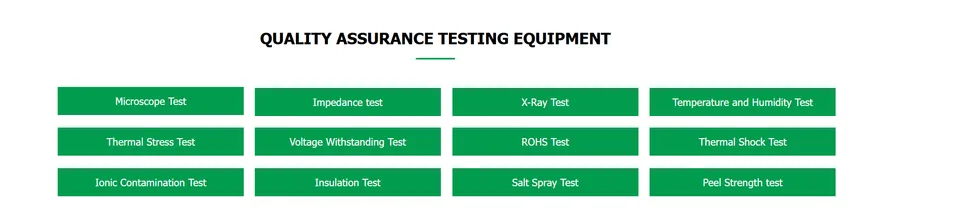
Published test coverage and process-control checkpoints across production.
01Microscope Test
02Impedance Test
03X-Ray Test
04Temperature and Humidity Test
05Thermal Stress Test
06Voltage Withstanding Test
07RoHS Test
08Thermal Shock Test
09Ionic Contamination Test
10Insulation Test
11Salt Spray Test
12Peel Strength Test
13PCB Electrical Testing
14Microsection Analysis
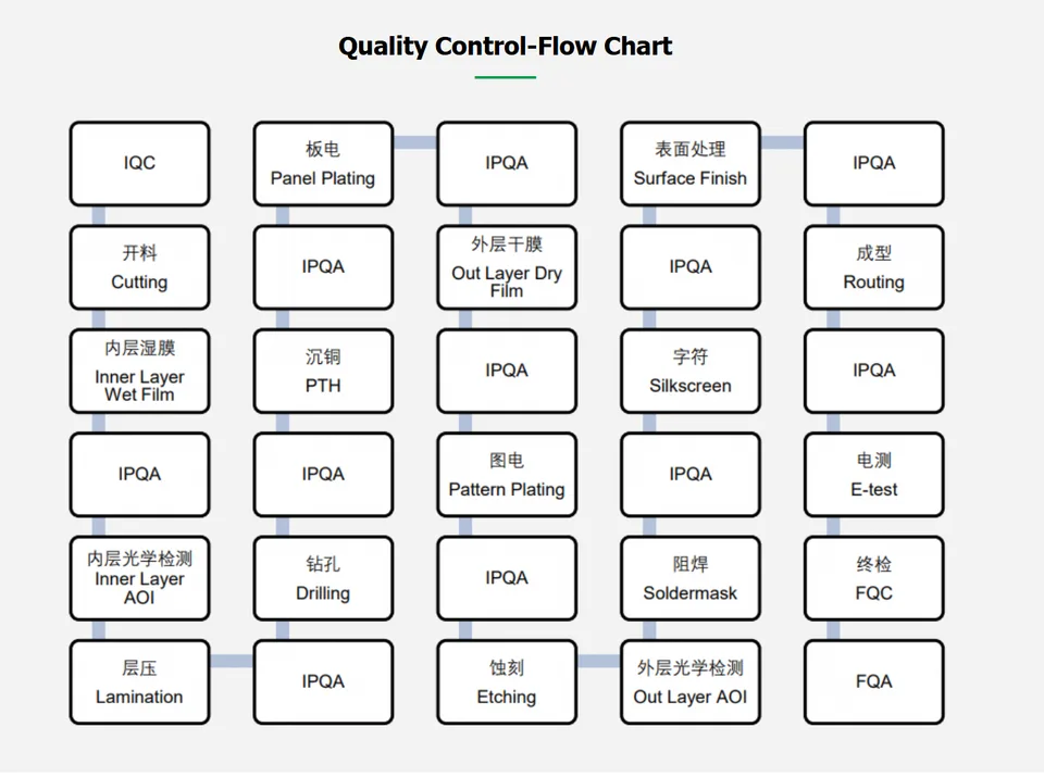
01Incoming Quality Control (IQC)→
02Cutting→
03Inner Layer Wet Film→
04In-Process Quality Assurance (IPQA)→
05Inner Layer AOI→
06Lamination→
07In-Process Quality Assurance (IPQA)→
08Drilling→
09In-Process Quality Assurance (IPQA)→
10PTH→
11In-Process Quality Assurance (IPQA)→
12Panel Plating→
13In-Process Quality Assurance (IPQA)→
14Outer Layer Dry Film→
15In-Process Quality Assurance (IPQA)→
16Pattern Plating→
17In-Process Quality Assurance (IPQA)→
18Etching→
19Outer Layer AOI→
20Solder Mask→
21In-Process Quality Assurance (IPQA)→
22Silkscreen→
23In-Process Quality Assurance (IPQA)→
24Surface Finish→
25In-Process Quality Assurance (IPQA)→
26Routing→
27In-Process Quality Assurance (IPQA)→
28E-Test→
29Final Quality Control (FQC)→
30Final Quality Assurance (FQA)→
Quality assurance testing equipment source chartQuality control flow source chart
DELIVERY / PAYMENT
완성된 보드부터 고객 입고 지점까지.
Choose your nominated forwarder or ask JETFGO to coordinate shipment. The confirmed carrier, Incoterm, insurance, charges and customs responsibilities are recorded in the quotation or proforma invoice before dispatch.
01 / CUSTOMER ROUTE
Use your own forwarder
Send the forwarder name, warehouse address, account number and booking instructions. We prepare the packing list, commercial documents and handover details required by the confirmed shipping term.
Customer accountWarehouse handover
02 / COORDINATED ROUTE
JETFGO coordinates delivery
We can request suitable express, air-cargo, sea-freight or other available routes based on destination, shipment size, urgency and customs requirements. Freight cost and responsibility are confirmed before shipment.
Air / expressSea freight
01Final inspection and release
02ESD / moisture / impact-safe packing
03Shipping documents and booking
04Tracking and delivery follow-up
Shipment confirmation checklist
01Route
Express, air, sea or another agreed service according to destination and shipment profile.
02Forwarder
Customer-nominated account or a route coordinated by JETFGO.
03Trade term
The selected Incoterm and each party’s responsibilities appear on the commercial document.
04Documents
Packing list, invoice and available origin or compliance documents are prepared as agreed.
COMMERCIAL SETTLEMENT
주요 결제 방법은 주문별로 확인합니다.
Bank transfer is commonly used for international PCB and PCBA orders. Card, digital-wallet and trade-finance options may be arranged when available for the customer, currency, region and order. Final payment instructions come only from an official JETFGO quotation or proforma invoice.
T/T
Bank Transfer / T/TPreferred for international orders. Use only the bank details shown on the official proforma invoice.Confirmed order by order
VisaAvailable only through an official card-payment link when stated on the quotation.Confirmed order by order
MastercardAvailable only through an official card-payment link when stated on the quotation.Confirmed order by order
UnionPayAvailable for supported regions and currencies after order confirmation.Confirmed order by order
American ExpressAvailable for eligible orders when included in the confirmed payment route.Confirmed order by order
PayPalAvailable only when PayPal is listed on the quotation or proforma invoice.Confirmed order by order
WeChat PayFor eligible RMB or regional transactions after confirmation by the sales team.Confirmed order by order
AlipayFor eligible RMB or regional transactions after confirmation by the sales team.Confirmed order by order
L/C
Letter of CreditFor qualifying orders subject to prior agreement on the issuing bank and L/C terms.Confirmed order by order
FACTORY VISIT
공장 방문을 요청하세요.
희망 날짜, 방문 인원, 확인할 생산·품질 영역을 알려주시면 담당자가 일정과 방문 계획을 확정합니다.
Submitting this form is a request, not an automatic booking. The visit is confirmed only after written confirmation from JETFGO.

 PRODUCT & PROCESS DETAIL
 01