
소형, 가동 또는 공간 제약 인터커넥트를 위한 폴리이미드 구조. 검증된 공정 범위: Flex layers: Up to 12 layers; Flex thickness: 0.1–1.0 mm; Flex materials: SHENGYI · Pyralux® KP · Panasonic 검토용 파일: Gerber 또는 ODB++, 드릴 파일, 스택업, 제작 도면, 수량 및 목표 일정. 게시된 한계는 JETFGO의 현재 공정 능력표를 기반으로 하며 최종 가능성은 전체 자료 검토 후 확정됩니다.
게시된 한계는 JETFGO의 현재 공정 능력표를 기반으로 하며 최종 가능성은 전체 자료 검토 후 확정됩니다.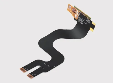
JETFGO / FLEX-MLFLEX
01 / 엔지니어링 답변
엔지니어링 답변
02 / DATA
검증된 공정 범위
소형, 가동 또는 공간 제약 인터커넥트를 위한 폴리이미드 구조.
Flex Layer Capability
Up to 12 layers
Flex Thickness Range
0.1–1.0 mm
Flex Material Options
SHENGYI · Pyralux® KP · Panasonic
Flex Application
Static or dynamic use, subject to project review
Flex-Zone Review
Bend area · routing direction · coverlay · stiffener
Engineering Review
Stack-up · copper structure · bend requirements · assembly interface
05 / INPUT
검토용 파일
Flex PCB Engineering Package
Gerber or ODB++, drill files, proposed stack-up, fabrication drawing, quantity, target delivery date and any defined bend, flex-zone, coverlay or stiffener requirements.
Flex Stack-up Requirements
Provide the proposed layer structure, flex thickness, copper weights, polyimide material requirements and any adhesive or coverlay specifications when available.
Bend & Flex-Zone Requirements
Identify static or dynamic use, bend locations, available bend radius, movement direction and any restricted component or plated-feature areas.
Stiffener & Assembly Requirements
견적 요청Provide stiffener locations, connector or component areas, assembly interfaces and any thickness requirements at reinforced sections.
06 / FAQ
기술 질문
게시된 한계는 JETFGO의 현재 공정 능력표를 기반으로 하며 최종 가능성은 전체 자료 검토 후 확정됩니다.
01What is a multilayer flexible PCB?+
A multilayer flexible PCB contains multiple conductive layers within a flexible polyimide-based structure, providing greater routing density while allowing the circuit to bend, fold or fit into compact assemblies.
02Which files help JETFGO review a multilayer flex PCB fastest?+
Send Gerber or ODB++, drill files, proposed stack-up, fabrication drawing, quantity, target delivery date and any defined bend, flex-zone, coverlay, stiffener or assembly requirements.
03Can JETFGO support prototypes and repeat production for multilayer flexible PCBs?+
Yes. Once the flex stack-up, materials, bend requirements and manufacturing conditions are confirmed, the approved engineering record can support prototype validation and repeat production under the same process conditions.
04What is the difference between a flexible PCB and a rigid-flex PCB?+
A flexible PCB uses flexible circuit construction throughout the relevant board area, while a rigid-flex PCB permanently combines rigid PCB sections and flexible interconnect sections within one integrated structure.
05Can multilayer flexible PCBs be used for dynamic bending?+
They can be evaluated for dynamic-flex applications, but final suitability depends on the flex stack-up, copper construction, bend radius, conductor routing, flex length and required movement cycle.
06What information is needed to define a flex PCB bend area?+
Provide the bend location, available bend radius, static or dynamic use, movement direction, flex-zone length and any restrictions on components, vias or plated features in the bending area.
07What are stiffeners used for on a flexible PCB?+
Stiffeners reinforce selected flex PCB areas such as connectors, component locations or assembly interfaces where additional mechanical support or controlled thickness is required.
08Does a higher flex layer count affect bending performance?+
Yes. Increasing the number of conductive and dielectric layers generally increases the mechanical complexity of the flex structure, so bend performance must be reviewed together with total thickness, copper construction and intended movement.
RFQ / DFM
요구사항을 보내고 실행 가능한 공급 계획을 받으세요.
Gerber 또는 ODB++, 적층, 재료, 수량, 목표 일정과 검사 요구를 보내주시면 기술 검토 후 견적합니다.
기술 검토소재·스택업정밀 제조