
20년 이상의 제조 전문성.
JETFGO Circuits는 2004년 선전에서 설립되어 PCB 시제품, 중소량 생산, PCBA 서비스를 제공합니다.
공장 직접 견적 요청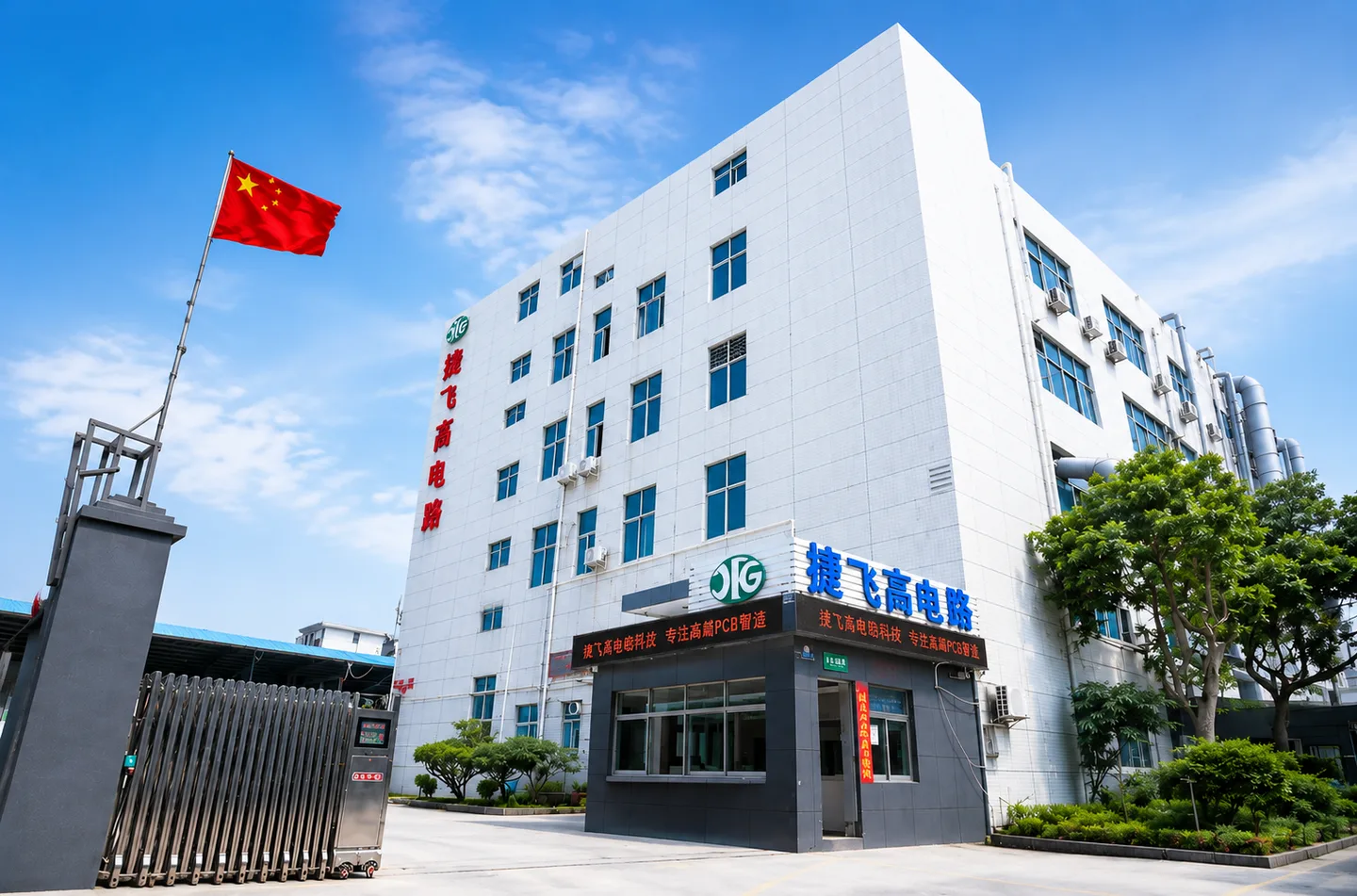 PRODUCT & PROCESS DETAIL
엔지니어가 JETFGO를 선택하는 이유
Founded in Shenzhen in 2004, JETFGO has grown around a straightforward manufacturing principle: customers should know who makes their PCBs and how they are produced. We own and operate our PCB manufacturing facilities, supported by dedicated engineering, production and quality teams. Our customers include electronics manufacturers, OEMs, EMS providers, distributors and international sourcing businesses.
Our manufacturing capabilities cover conventional multilayer PCBs, HDI, high-speed and RF circuits, flexible and rigid-flex boards, as well as PCB assembly services. We evaluate customer-provided Gerber files, stackups, materials and production requirements before manufacturing. From engineering prototypes to repeat orders, our focus is on practical DFM support, defined process controls and consistent manufacturing quality.
Working directly with JETFGO gives sourcing teams access to the factory responsible for manufacturing their boards. We support small prototype quantities without a fixed MOQ, specialized PCB requirements and flexible production planning. For companies with established suppliers, we can also serve as a second manufacturing source for new projects, urgent builds or capacity backup, without requiring them to replace existing partners.
인증된 공정. 측정 가능한 관리.
통제된 공정과 엄격한 검사가 복잡한 설계를 반복 가능한 생산으로 전환합니다.
요구사항을 보내고 실행 가능한 공급 계획을 받으세요.
Gerber 또는 ODB++, 적층, 재료, 수량, 목표 일정과 검사 요구를 보내주시면 기술 검토 후 견적합니다.