
 PRODUCT & PROCESS DETAIL
JETFGOが選ばれる理由
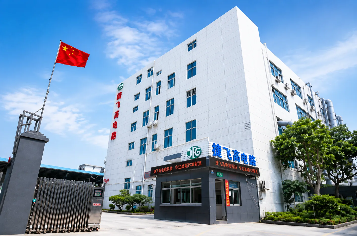
Founded in Shenzhen in 2004, JETFGO has grown around a straightforward manufacturing principle: customers should know who makes their PCBs and how they are produced. We own and operate our PCB manufacturing facilities, supported by dedicated engineering, production and quality teams. Our customers include electronics manufacturers, OEMs, EMS providers, distributors and international sourcing businesses.
Our manufacturing capabilities cover conventional multilayer PCBs, HDI, high-speed and RF circuits, flexible and rigid-flex boards, as well as PCB assembly services. We evaluate customer-provided Gerber files, stackups, materials and production requirements before manufacturing. From engineering prototypes to repeat orders, our focus is on practical DFM support, defined process controls and consistent manufacturing quality.
Working directly with JETFGO gives sourcing teams access to the factory responsible for manufacturing their boards. We support small prototype quantities without a fixed MOQ, specialized PCB requirements and flexible production planning. For companies with established suppliers, we can also serve as a second manufacturing source for new projects, urgent builds or capacity backup, without requiring them to replace existing partners.
認証工程と数値で管理する品質。
管理された工程と厳格な検査により、複雑な設計データを再現性の高い製品へ変えます。
要件を送り、実行可能な供給計画を受け取る。
Gerber または ODB++、積層、材料、数量、希望納期、検査要件をお送りください。技術確認後に見積します。