
コネクタ削減と移行部管理を両立する一体型リジッドフレックス。 確認済み工程範囲: Flex capability: Up to 12 layers; Blind / laser via: 3–5 mil; IPC class: Class 2 and Class 3 レビュー用資料: GerberまたはODB++、ドリルデータ、層構成、製造図、数量、希望納期。 掲載値はJETFGOの現行工程能力表に基づきます。最終可否は完全な設計資料で確認します。
掲載値はJETFGOの現行工程能力表に基づきます。最終可否は完全な設計資料で確認します。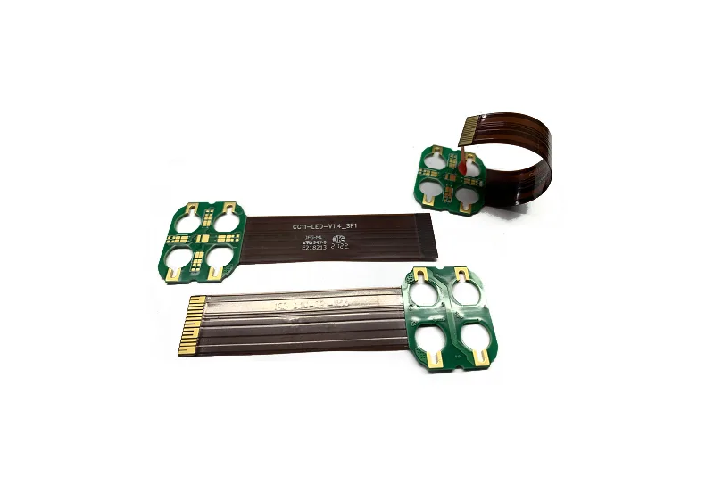
JETFGO / RFX-06LRIGID-FLEX
01 / 技術回答
技術回答
02 / DATA
確認済み工程範囲
コネクタ削減と移行部管理を両立する一体型リジッドフレックス。
Flex Layer Capability
Up to 12 layers
Blind / Laser Microvia
3–5 mil
IPC Workmanship Class
Class 2 and Class 3, subject to project requirements
Rigid-Flex Structure
Integrated rigid regions · flexible interconnect zones
Flex-Zone Review
Bend area · transition · coverlay · stiffener · copper routing
Engineering Review
Stack-up · via structure · bend requirements · assembly interface
05 / INPUT
レビュー用資料
Rigid-Flex Engineering Package
Gerber or ODB++, drill files, proposed rigid-flex stack-up, fabrication drawing, quantity, target delivery date and any bend, flex-zone, via, coverlay, stiffener or IPC-class requirements.
Rigid-Flex Stack-up Requirements
Provide the rigid and flex layer structure, board thicknesses, flex thickness, copper weights, polyimide material requirements and layer-transition information.
Bend & Flex-Zone Requirements
Identify bend locations, available bend radius, static or dynamic use, flex-zone length, movement direction and any restricted component or via areas.
Transition & Reinforcement Requirements
Provide rigid-to-flex transition locations, coverlay requirements, stiffener locations, connector interfaces and any mechanical reinforcement requirements.
IPC & Reliability Requirements
見積もり依頼Specify the required IPC workmanship class, inspection criteria and any project-specific reliability, qualification or documentation requirements.
06 / FAQ
技術FAQ
掲載値はJETFGOの現行工程能力表に基づきます。最終可否は完全な設計資料で確認します。
01What is a 6-layer rigid-flex PCB?+
A 6-layer rigid-flex PCB combines rigid PCB regions and flexible interconnect sections within one integrated circuit structure. It can reduce connectors and cable assemblies while supporting compact packaging and controlled flex routing.
02Which files help JETFGO review a 6-layer rigid-flex PCB fastest?+
Send Gerber or ODB++, drill files, proposed rigid-flex stack-up, fabrication drawing, quantity, target delivery date and any bend, flex-zone, via, coverlay, stiffener or IPC-class requirements.
03Can JETFGO support prototypes and repeat production for rigid-flex PCBs?+
Yes. Once the rigid-flex stack-up, materials, via structure, bend requirements and manufacturing conditions are confirmed, the approved engineering record can support prototype validation and repeat production.
04What is the difference between rigid-flex PCB and flexible PCB?+
A flexible PCB primarily uses flexible circuit construction, while a rigid-flex PCB permanently combines rigid PCB sections and flexible interconnect sections within the same integrated board structure.
05Why use a rigid-flex PCB instead of separate PCBs and cables?+
Rigid-flex construction can reduce connectors, cables and separate interconnect assemblies while improving packaging efficiency. Final benefits depend on the mechanical, electrical and assembly requirements of the product.
06Can blind or laser microvias be used in a rigid-flex PCB?+
Yes. Blind and laser-drilled microvias can be evaluated for rigid-flex designs when higher routing density is required. Final feasibility depends on the layer structure, via location, transition regions and complete manufacturing stack-up.
07Can JETFGO manufacture rigid-flex PCBs to IPC Class 3 requirements?+
JETFGO can review rigid-flex projects requiring IPC Class 2 or Class 3 workmanship. Final process controls, inspection requirements and qualification conditions are confirmed according to the complete project specification.
08What should be considered in the rigid-to-flex transition area?+
The transition area should be reviewed for copper routing, dielectric changes, coverlay, bend location, via placement, mechanical stress and component clearance to reduce reliability risks during assembly and use.
RFQ / DFM
要件を送り、実行可能な供給計画を受け取る。
Gerber または ODB++、積層、材料、数量、希望納期、検査要件をお送りください。技術確認後に見積します。
技術レビュー材料・層構成精密製造