
 PRODUCT & PROCESS DETAIL
PCB Manufacturing for Compact and Connected Devices
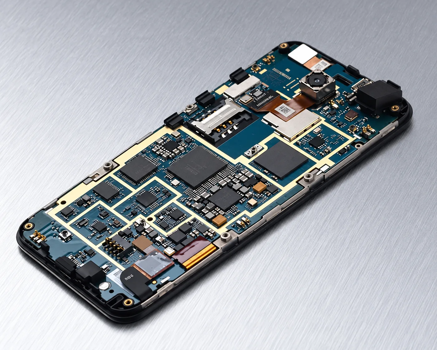
Consumer electronics increasingly integrate processors, wireless connectivity, sensors and power management into compact assemblies. JETFGO supports multilayer, HDI, flexible and rigid-flex PCB manufacturing for smart home products, wearable technology, IoT modules and portable electronic devices. Engineering review covers PCB density, material selection, signal routing and assembly manufacturability.
기술 솔루션 디렉터리
각 페이지는 하나의 구체적 요구에 대해 검증 가능한 공정 범위와 검토 자료를 제시합니다.
1+N+1 HDI Microvia PCB
A high-density PCB manufacturing solution for compact consumer electronics, smart wearables, IoT controllers and embedded processing modules. The 1+N+1 HDI construction supports laser-drilled microvias, fine-pitch component routing and dense multilayer interconnections. Engineering review covers BGA fan-out, via construction, dielectric selection, layer stack-up and manufacturing feasibility.
솔루션 보기FLEX-MLMultilayer Flexible PCB
A multilayer flexible PCB manufacturing solution for wearable devices, portable electronics, smart sensors and compact consumer hardware. Polyimide construction supports space-efficient electrical interconnections within curved or restricted mechanical assemblies. Engineering review covers material selection, copper thickness, bend radius, layer construction and assembly integration.
솔루션 보기PCBA-BOXTurnkey PCBA & Box Build
An integrated PCB and PCBA manufacturing solution for smart home electronics, IoT devices, wearable modules and connected consumer hardware. JETFGO coordinates PCB fabrication, BOM-based component sourcing, SMT assembly, through-hole assembly, inspection, customer-defined testing and final assembly. Product firmware and finished-device certification remain customer responsibilities.
솔루션 보기RFX-06L6-Layer Rigid-Flex PCB
A six-layer rigid-flex PCB manufacturing solution for compact smart devices, portable instruments, wearable modules and miniature electronic assemblies. Integrated rigid and flexible regions can reduce separate connector requirements and improve packaging flexibility. Engineering review includes layer construction, material selection, rigid-to-flex transitions and mechanical integration.
솔루션 보기QT-24HQuick-Turn PCB Prototype
A quick-turn PCB prototyping solution for smart hardware startups, IoT product development, wearable electronics and consumer device engineering validation. JETFGO supports prototype fabrication, DFM review and manufacturing feedback before repeat production. Lead times depend on design complexity, material availability and engineering confirmation.
솔루션 보기SI-04L4-Layer Controlled-Impedance PCB
A four-layer controlled-impedance PCB manufacturing solution for smart home controllers, wireless IoT interfaces, sensor modules and embedded consumer electronics. Engineering review covers multilayer stack-up, differential signal routing, reference-plane continuity, dielectric selection and impedance tolerances.
솔루션 보기요구사항을 보내고 실행 가능한 공급 계획을 받으세요.
Gerber 또는 ODB++, 적층, 재료, 수량, 목표 일정과 검사 요구를 보내주시면 기술 검토 후 견적합니다.