
Applications

Consumer Electronics & Smart Hardware PCB Manufacturing

PCB manufacturing and PCBA assembly for consumer electronics, smart home devices, IoT products and wearable technology. JETFGO supports multilayer, HDI, flexible and rigid-flex PCBs, with component sourcing, SMT assembly and manufacturing services from prototypes to repeat production.

Get a factory-direct quote
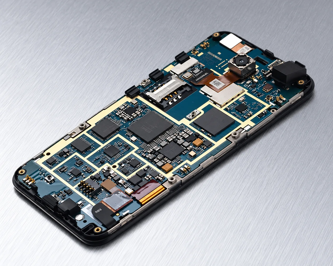
JETFGO / Consumer Electronics & Smart Hardware PCB ManufacturingConsumer Electronics & Smart Hardware PCB ManufacturingPRODUCT & PROCESS DETAIL
CONSUMER ELECTRONICS & SMART HARDWARE

PCB Manufacturing for Compact and Connected Devices

Consumer electronics increasingly integrate processors, wireless connectivity, sensors and power management into compact assemblies. JETFGO supports multilayer, HDI, flexible and rigid-flex PCB manufacturing for smart home products, wearable technology, IoT modules and portable electronic devices. Engineering review covers PCB density, material selection, signal routing and assembly manufacturability.

PCB material and stack-up engineering for compact consumer electronics, including FR-4 laminates, polyimide flexible materials, copper thickness, dielectric properties, board thickness and multilayer construction for space-constrained devices.Controlled-impedance and high-density PCB manufacturing for wireless modules, embedded processors and smart device interfaces, including reference-plane continuity, differential signal routing, fine-pitch interconnections and multilayer stack-up requirements.Manufacturing traceability and inspection controls covering PCB material identification, BOM verification, component sourcing, AOI, electrical testing, assembly inspection and customer-defined quality acceptance requirements.Prototype-to-repeat-production manufacturing support through DFM review, approved fabrication data, controlled BOM revisions, SMT assembly documentation, component sourcing coordination and consistent inspection requirements for consumer electronics projects.HDI PCB manufacturing for compact smart devices, including laser-drilled microvias, fine-pitch BGA routing, sequential lamination, high-density interconnections and multilayer stack-up evaluation.Flexible PCB engineering for wearable and portable electronics, covering polyimide materials, copper construction, bend radius, strain relief, conductor orientation and mechanical integration. Repeated bending applications require dedicated fatigue-life evaluation.Rigid-flex PCB construction for miniature smart hardware, including integrated rigid and flexible regions, connector reduction, rigid-to-flex transitions, multilayer interconnections and three-dimensional packaging requirements.PCB manufacturing review for IoT wireless communication modules, including RF trace geometry, dielectric material selection, controlled impedance, reference planes, antenna interface routing and manufacturing tolerances. Wireless certification requires separate product-level validation.SMT assembly review for high-density consumer electronics, including fine-pitch ICs, small passive components, BGA packages, component placement accuracy, solder paste requirements and inspection accessibility.High-speed PCB manufacturing for embedded processing and multimedia electronics, covering differential routing, impedance control, reference-plane continuity, multilayer stack-up construction and fine-pitch processor interconnections.PCB fabrication and PCBA assembly review for battery-powered smart devices, including power-management circuits, charging interfaces, battery monitoring electronics, conductor geometry and thermal considerations. Battery safety and charging performance require system-level verification.PCB manufacturing for compact sensing electronics, including environmental sensors, motion sensors, proximity sensors, touch interfaces and wearable measurement modules. Engineering review covers component density, grounding, signal routing and assembly requirements.Manufacturing considerations for EMI/EMC-sensitive smart hardware, including power-and-signal separation, grounding structures, reference-plane continuity, controlled-impedance routing and shielding interface requirements. Final compliance requires product-level testing.Mechanical and dimensional PCB manufacturing review for lightweight consumer devices, including board thickness, outline tolerances, mounting-hole positions, connector clearances, component height restrictions and enclosure integration.PCB and PCBA manufacturing quality controls including incoming material inspection, AOI, electrical testing, component verification and agreed functional testing. Inspection criteria and test coverage are established according to customer-approved requirements.BOM-based sourcing and component traceability for smart hardware manufacturing, including approved manufacturer part numbers, material availability review, alternate-component approval, production revision control and sourcing coordination.Prototype and NPI manufacturing support for consumer electronics, including DFM feedback, PCB fabrication, SMT assembly, engineering change management, inspection requirements and controlled transitions into repeat production.Manufacturing review against customer-defined IPC acceptance requirements, material specifications and inspection criteria. Finished-device electrical safety, battery compliance, radio certification, environmental testing and market-access approval remain separate product-level responsibilities.
Solutions

Customer-requirement solution directory

Each page turns one common customer need into a clear manufacturing route, published capability limits and an RFQ file checklist your team can reuse.

HDI-1N1

1+N+1 HDI Microvia PCB

A high-density PCB manufacturing solution for compact consumer electronics, smart wearables, IoT controllers and embedded processing modules. The 1+N+1 HDI construction supports laser-drilled microvias, fine-pitch component routing and dense multilayer interconnections. Engineering review covers BGA fan-out, via construction, dielectric selection, layer stack-up and manufacturing feasibility.

Open solution
FLEX-ML

Multilayer Flexible PCB

A multilayer flexible PCB manufacturing solution for wearable devices, portable electronics, smart sensors and compact consumer hardware. Polyimide construction supports space-efficient electrical interconnections within curved or restricted mechanical assemblies. Engineering review covers material selection, copper thickness, bend radius, layer construction and assembly integration.

Open solution
PCBA-BOX

Turnkey PCBA & Box Build

An integrated PCB and PCBA manufacturing solution for smart home electronics, IoT devices, wearable modules and connected consumer hardware. JETFGO coordinates PCB fabrication, BOM-based component sourcing, SMT assembly, through-hole assembly, inspection, customer-defined testing and final assembly. Product firmware and finished-device certification remain customer responsibilities.

Open solution
RFX-06L

6-Layer Rigid-Flex PCB

A six-layer rigid-flex PCB manufacturing solution for compact smart devices, portable instruments, wearable modules and miniature electronic assemblies. Integrated rigid and flexible regions can reduce separate connector requirements and improve packaging flexibility. Engineering review includes layer construction, material selection, rigid-to-flex transitions and mechanical integration.

Open solution
QT-24H

Quick-Turn PCB Prototype

A quick-turn PCB prototyping solution for smart hardware startups, IoT product development, wearable electronics and consumer device engineering validation. JETFGO supports prototype fabrication, DFM review and manufacturing feedback before repeat production. Lead times depend on design complexity, material availability and engineering confirmation.

Open solution
SI-04L

4-Layer Controlled-Impedance PCB

A four-layer controlled-impedance PCB manufacturing solution for smart home controllers, wireless IoT interfaces, sensor modules and embedded consumer electronics. Engineering review covers multilayer stack-up, differential signal routing, reference-plane continuity, dielectric selection and impedance tolerances.

Open solution
RFQ / DFM

Discuss your next order directly with our factory.

Send the Gerber or ODB++, stackup, material, quantity, target date and test requirements. Our team will review feasibility and return a technical quotation for the order you manage.

Engineering reviewMaterial & stackupPrecision fabrication