
Hybrid PCB Engineering Review
Our engineering team reviews hybrid PCB requirements including material combinations, stack-up structures, layer configurations and manufacturing feasibility before production to ensure reliable fabrication.
Hybrid PCBs combine RF laminates and FR-4 within one board for applications needing different electrical material properties. JETFGO reviews mixed-material stack-ups for high-frequency and high-speed projects before fabrication. JETFGO operates its own PCB manufacturing facilities in Shenzhen, China. Our engineering team evaluates hybrid PCB stack-up structures, material compatibility and manufacturing feasibility before production.
Get a factory-direct quote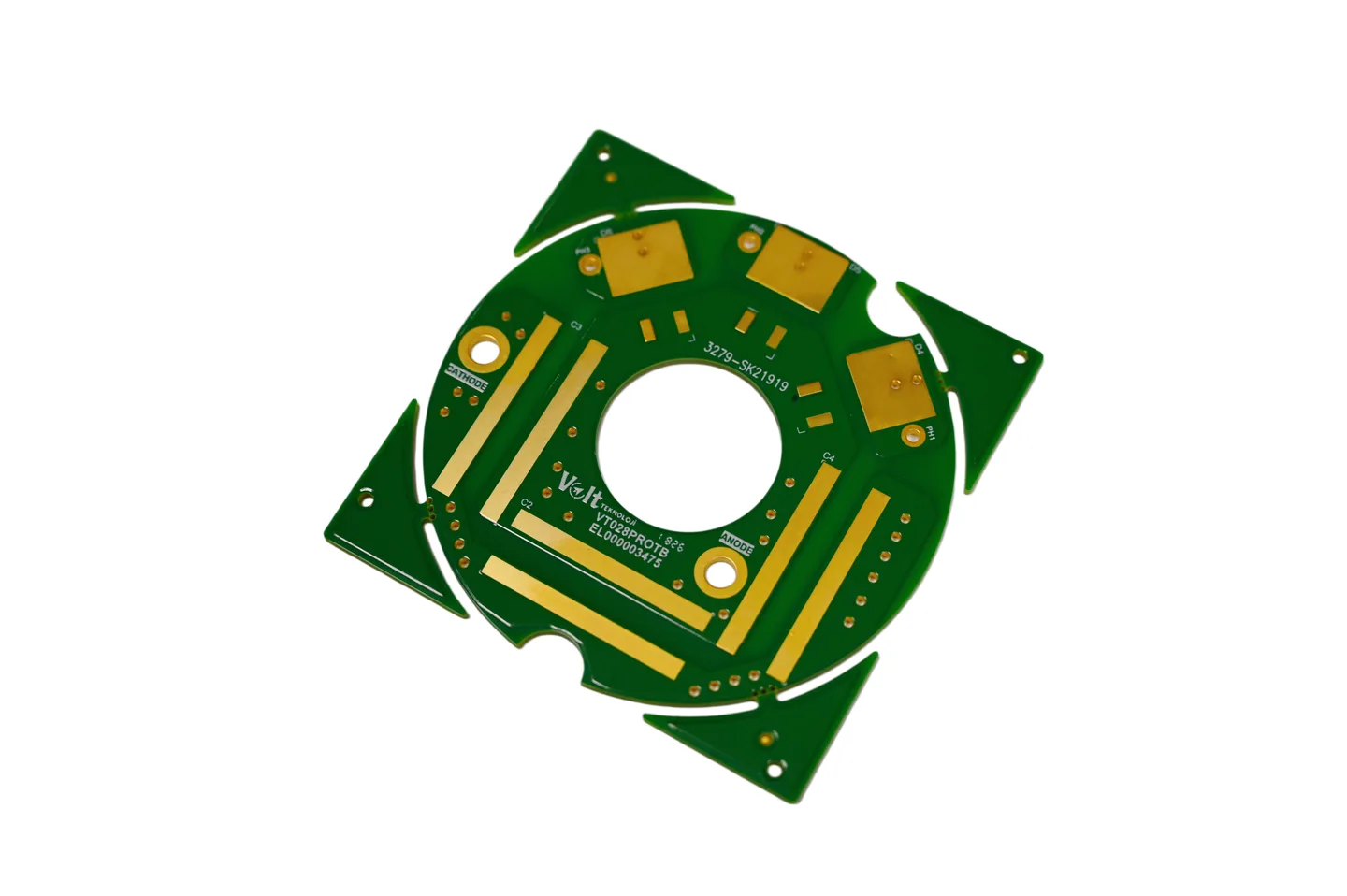 PRODUCT & PROCESS DETAIL
JETFGO is a Shenzhen-based hybrid PCB manufacturer specializing in mixed-material PCB solutions that combine different laminate technologies within a single board structure. Our factory supports hybrid PCB manufacturing using RF materials, high-frequency laminates and standard FR-4 materials to achieve balanced electrical performance, cost efficiency and design flexibility. Hybrid PCB solutions are widely used in RF modules, communication equipment, radar systems, antenna applications and other electronic products requiring different material properties within one PCB design. From prototype development to volume production, JETFGO provides engineering support including material evaluation, stack-up review and manufacturing process control.
Buy directly from the manufacturer. Our own factory teams review DFM, plan production and inspect your boards, with equipment and process records available for supplier qualification.
Our engineering team reviews hybrid PCB requirements including material combinations, stack-up structures, layer configurations and manufacturing feasibility before production to ensure reliable fabrication.
JETFGO supports hybrid PCB projects by evaluating RF laminates, FR-4 materials and mixed dielectric structures to achieve balanced electrical performance, reliability and cost efficiency.
Our manufacturing process supports mixed-material PCB fabrication with controlled lamination, accurate layer alignment and reliable bonding between different PCB materials.
JETFGO applies material verification, AOI inspection, electrical testing and process traceability to ensure stable performance and reliability of hybrid PCB products.
JETFGO integrates RF materials and standard PCB materials within one hybrid structure to support applications requiring both high-frequency performance and cost control.
From prototype validation to volume manufacturing, JETFGO provides flexible hybrid PCB production support with engineering assistance throughout the project lifecycle.
Hybrid PCB solutions support applications requiring different electrical characteristics, including RF performance, signal integrity and mechanical reliability.
Learn about hybrid PCB materials, mixed stack-up structures, manufacturing capability and production requirements.
Customers can provide Gerber files or ODB++, stack-up information, material requirements, layer count, quantity and surface finish requirements. Our engineering team will evaluate the hybrid PCB structure before quotation.
Yes. JETFGO supports hybrid PCB prototypes, NPI projects and volume production. Our engineering team provides support from material evaluation and stack-up design to final manufacturing.
Hybrid PCB quality is verified through material inspection, lamination control, AOI inspection, electrical testing and production traceability to ensure reliable performance.
A hybrid PCB combines different PCB materials, such as RF laminates and FR-4, within one board structure to achieve specific electrical, mechanical and cost requirements.
Mixed-material PCB stack-ups allow designers to combine different material properties, such as high-frequency performance, signal integrity and cost efficiency, within one PCB design.
Yes. JETFGO supports hybrid PCB manufacturing by combining RF laminates and FR-4 materials based on electrical requirements, application needs and manufacturing feasibility.
Hybrid PCBs are commonly used in RF modules, radar systems, communication equipment, antenna systems and other electronic products requiring different material characteristics.
JETFGO operates its PCB manufacturing facility in Shenzhen, China, providing hybrid PCB fabrication and PCBA manufacturing support for global customers.
Send the Gerber or ODB++, stackup, material, quantity, target date and test requirements. Our team will review feasibility and return a technical quotation for the order you manage.