HDI PCB Manufacturing CapabilityConfirm manufacturing fit before you quote your customer.
JETFGO is a Shenzhen-based HDI PCB manufacturer specializing in high-density interconnect PCB solutions for advanced electronic applications.
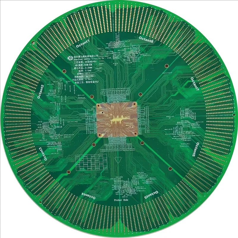
Our factory supports HDI PCB manufacturing from engineering review and stack-up optimization to prototype validation, NPI and volume production. With advanced technologies including microvia, sequential lamination, laser drilling and fine-line routing, we help customers build compact, reliable and high-performance electronic products.
JETFGO provides HDI PCB solutions for industrial electronics, automotive systems, AI servers, medical devices, semiconductor equipment and communication applications.
BuildAny-layer HDI · Sequential lamination · mSAP technology · Multilayer HDI structures
MicroviaLaser microvia ≤ 0.15 mm · Reliable interconnection for high-density PCB designs
Fine Line / Space Capability40 μm / 40 μm fine line and spacing capability
Solder mask registration±1 mil solder mask registration accuracy for precise HDI PCB manufacturing
Layer CountUp to 60 layers multilayer PCB capability
PCB MaterialHigh-speed materials, low-loss laminates and advanced PCB substrates
Surface FinishENIG, immersion gold and other production finishes available
Testing CapabilityAOI inspection, electrical testing, impedance control and production traceability
Typical HDI PCB ApplicationsHigh-density PCB Solutions for Advanced Electronics
JETFGO HDI PCB solutions are used in compact and high-performance electronic systems requiring reliable interconnection, signal integrity and space optimization.
HDI PCB Manufacturing FAQCommon Questions About HDI PCB Production
Find answers about HDI PCB technology, manufacturing capability, required files, production process and engineering support.
06Common Questions About HDI PCB Production
01What files are required for HDI PCB manufacturing?+
Customers can provide Gerber files or ODB++, fabrication drawings, stack-up information, PCB quantity, material requirements and surface finish requirements. Our engineering team can review the design before quotation and production.
02Can JETFGO support prototype and volume HDI PCB production?+
Yes. JETFGO supports prototype, NPI and low-to-medium volume HDI PCB manufacturing. Our factory can support customers from initial validation to stable production without MOQ requirements.
03How is quality verified?+
Quality is controlled through incoming material inspection, AOI inspection, electrical testing, impedance control and production traceability. Quality requirements can also be customized based on project needs.
04What HDI PCB technologies can you manufacture?+
JETFGO supports advanced HDI technologies including laser microvias, sequential lamination, any-layer HDI, fine-line routing and multilayer PCB manufacturing.
05Where is your HDI PCB factory located?+
JETFGO operates its PCB manufacturing facility in Shenzhen, China. We provide HDI PCB fabrication, PCB assembly and manufacturing support for global customers.
06Can JETFGO manufacture HDI PCB for AI and high-speed applications?+
Yes. Our HDI PCB capabilities support advanced applications including AI servers, high-speed computing, semiconductor equipment, industrial electronics and communication systems.

 PRODUCT & PROCESS DETAIL