
예측 가능한 단일 종단 또는 차동 임피던스를 위한 실용적 스택업. 검증된 공정 범위: Impedance tolerance: ±8%; Line / spacing example: Minimum 3 / 2.5 mil; Materials: TG135–TG180 FR-4 options 검토용 파일: Gerber 또는 ODB++, 드릴 파일, 스택업, 제작 도면, 수량 및 목표 일정. 게시된 한계는 JETFGO의 현재 공정 능력표를 기반으로 하며 최종 가능성은 전체 자료 검토 후 확정됩니다.
게시된 한계는 JETFGO의 현재 공정 능력표를 기반으로 하며 최종 가능성은 전체 자료 검토 후 확정됩니다.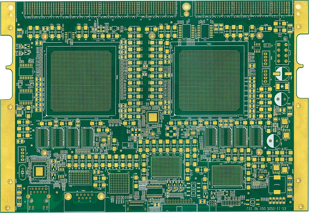
JETFGO / SI-04LRIGID
01 / 엔지니어링 답변
엔지니어링 답변
02 / DATA
검증된 공정 범위
예측 가능한 단일 종단 또는 차동 임피던스를 위한 실용적 스택업.
Impedance Tolerance
±8%
Minimum Line / Space
3 / 2.5 mil
FR-4 Material Options
Tg135–Tg180 FR-4
Impedance Types
Single-ended · differential
Stack-up Review
Routing layer · reference plane · dielectric · copper geometry
05 / INPUT
검토용 파일
Controlled-Impedance Engineering Package
Gerber or ODB++, drill files, proposed stack-up, fabrication drawing, quantity, target delivery date and applicable controlled-impedance requirements.
Impedance Requirement Table
For each controlled signal class, provide the target impedance, tolerance, routing layer, reference plane and whether manufacturer trace-width adjustment is permitted.
Stack-up & Material Requirements
견적 요청Provide the preferred layer structure, board thickness, copper weight, FR-4 Tg or material preference and any dielectric requirements related to impedance control.
06 / FAQ
기술 질문
게시된 한계는 JETFGO의 현재 공정 능력표를 기반으로 하며 최종 가능성은 전체 자료 검토 후 확정됩니다.
01Is ±8% impedance tolerance guaranteed for every 4-layer PCB?+
No. ±8% is a published capability reference for this solution. Final feasibility depends on the complete stack-up, materials, copper thickness, trace geometry, target impedance and other project requirements confirmed during engineering review.
02Which files help JETFGO review a 4-layer controlled impedance PCB fastest?+
Send Gerber or ODB++, drill files, proposed stack-up, fabrication drawing, quantity, target delivery date and an impedance requirement table showing target values, tolerances, routing layers and reference planes.
03Can JETFGO support prototypes and repeat production for controlled impedance PCBs?+
Yes. Once the stack-up, materials and impedance requirements are confirmed, the approved engineering record can support prototype validation and repeat production under the same manufacturing conditions.
04What information is required for controlled impedance PCB manufacturing?+
For each controlled signal class, provide the target impedance, tolerance, routing layer and reference plane. The proposed stack-up, board thickness, copper requirements and material preference should also be included when available.
05Can a 4-layer PCB support both single-ended and differential impedance?+
Yes, when the stack-up, reference planes, dielectric structure and trace geometry are designed appropriately. Final manufacturability is confirmed after reviewing the complete PCB data and impedance requirements.
06Why is the reference plane important for controlled impedance?+
A continuous reference plane provides a defined return path and forms part of the transmission-line geometry that determines impedance. Plane gaps or changes can create impedance discontinuities and affect signal integrity.
RFQ / DFM
요구사항을 보내고 실행 가능한 공급 계획을 받으세요.
Gerber 또는 ODB++, 적층, 재료, 수량, 목표 일정과 검사 요구를 보내주시면 기술 검토 후 견적합니다.
기술 검토소재·스택업정밀 제조