
Empilage pratique pour une impédance simple ou différentielle prévisible. Fenêtre de procédé vérifiée: Impedance tolerance: ±8%; Line / spacing example: Minimum 3 / 2.5 mil; Materials: TG135–TG180 FR-4 options Fichiers pour la revue: Gerber ou ODB++, perçage, empilage, plan de fabrication, quantité et date cible. Les limites publiées proviennent de la matrice de capacités JETFGO. La faisabilité finale exige le dossier complet.
Les limites publiées proviennent de la matrice de capacités JETFGO. La faisabilité finale exige le dossier complet.Code solutionSI-04LCapacité vérifiée
PCB 4 couches à impédance contrôlée
Empilage pratique pour une impédance simple ou différentielle prévisible.
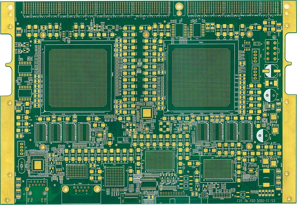
JETFGO / SI-04LRIGID
01 / RÉPONSE TECHNIQUE
Réponse technique
02 / DATA
Fenêtre de procédé vérifiée
Empilage pratique pour une impédance simple ou différentielle prévisible.
Impedance Tolerance
±8%
Minimum Line / Space
3 / 2.5 mil
FR-4 Material Options
Tg135–Tg180 FR-4
Impedance Types
Single-ended · differential
Stack-up Review
Routing layer · reference plane · dielectric · copper geometry
05 / INPUT
Fichiers pour la revue
Controlled-Impedance Engineering Package
Gerber or ODB++, drill files, proposed stack-up, fabrication drawing, quantity, target delivery date and applicable controlled-impedance requirements.
Impedance Requirement Table
For each controlled signal class, provide the target impedance, tolerance, routing layer, reference plane and whether manufacturer trace-width adjustment is permitted.
Stack-up & Material Requirements
Demander un devisProvide the preferred layer structure, board thickness, copper weight, FR-4 Tg or material preference and any dielectric requirements related to impedance control.
06 / FAQ
Questions techniques
Les limites publiées proviennent de la matrice de capacités JETFGO. La faisabilité finale exige le dossier complet.
01Is ±8% impedance tolerance guaranteed for every 4-layer PCB?+
No. ±8% is a published capability reference for this solution. Final feasibility depends on the complete stack-up, materials, copper thickness, trace geometry, target impedance and other project requirements confirmed during engineering review.
02Which files help JETFGO review a 4-layer controlled impedance PCB fastest?+
Send Gerber or ODB++, drill files, proposed stack-up, fabrication drawing, quantity, target delivery date and an impedance requirement table showing target values, tolerances, routing layers and reference planes.
03Can JETFGO support prototypes and repeat production for controlled impedance PCBs?+
Yes. Once the stack-up, materials and impedance requirements are confirmed, the approved engineering record can support prototype validation and repeat production under the same manufacturing conditions.
04What information is required for controlled impedance PCB manufacturing?+
For each controlled signal class, provide the target impedance, tolerance, routing layer and reference plane. The proposed stack-up, board thickness, copper requirements and material preference should also be included when available.
05Can a 4-layer PCB support both single-ended and differential impedance?+
Yes, when the stack-up, reference planes, dielectric structure and trace geometry are designed appropriately. Final manufacturability is confirmed after reviewing the complete PCB data and impedance requirements.
06Why is the reference plane important for controlled impedance?+
A continuous reference plane provides a defined return path and forms part of the transmission-line geometry that determines impedance. Plane gaps or changes can create impedance discontinuities and affect signal integrity.
RFQ / DFM
Envoyez le besoin. Recevez un plan d’approvisionnement fabricable.
Envoyez Gerber ou ODB++, empilage, matériaux, quantité, date cible et tests pour étude et devis technique.
Revue techniqueMatériaux et empilageFabrication précise