
긴급 설계 검증과 양산 전환을 위한 DFM 중심 시제품 경로. 검증된 공정 범위: Layer range: Engineering review up to 60-layer rigid PCB; Fine line example: Minimum 3 / 2.5 mil; Inspection: AOI · flying probe · electrical test 검토용 파일: Gerber 또는 ODB++, 드릴 파일, 스택업, 제작 도면, 수량 및 목표 일정. 게시된 한계는 JETFGO의 현재 공정 능력표를 기반으로 하며 최종 가능성은 전체 자료 검토 후 확정됩니다.
게시된 한계는 JETFGO의 현재 공정 능력표를 기반으로 하며 최종 가능성은 전체 자료 검토 후 확정됩니다.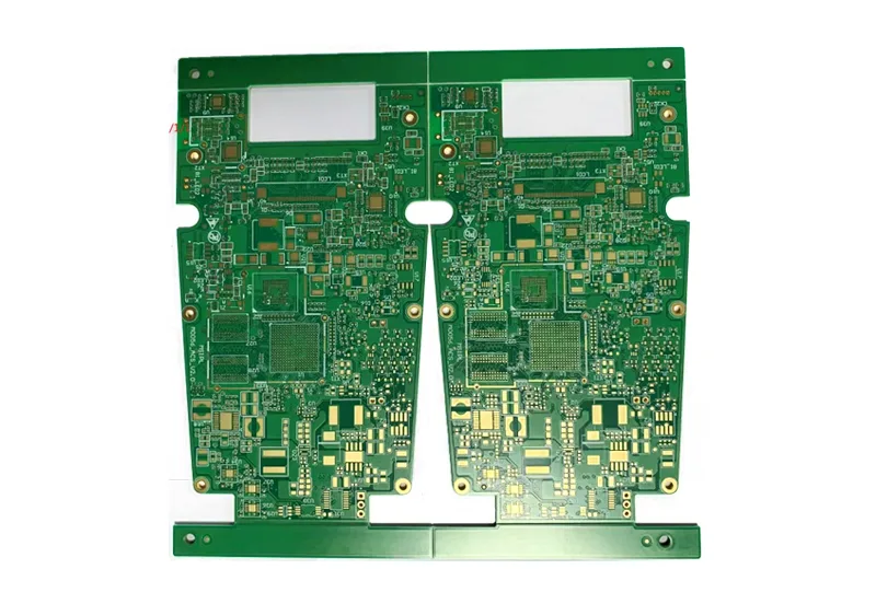
JETFGO / QT-24HRIGID
01 / 엔지니어링 답변
엔지니어링 답변
02 / DATA
검증된 공정 범위
긴급 설계 검증과 양산 전환을 위한 DFM 중심 시제품 경로.
Prototype Layer Capability
Engineering review up to 60-layer rigid PCB
Minimum Line / Space
3 / 2.5 mil
Inspection & Testing
AOI · flying probe · electrical test
Quick-Turn Lead Time
Confirmed after DFM, material availability and production-capacity review
Prototype Quantity
From 1 piece, subject to project review
05 / INPUT
검토용 파일
Quick-Turn PCB Review Package
Gerber or ODB++, drill files, proposed stack-up, fabrication drawing, quantity, target delivery date and any impedance, HDI or special-process requirements.
Quick-Turn Readiness Information
견적 요청Provide final revision files, required quantity, board thickness, copper weight, surface finish, solder-mask requirements and target delivery date to reduce quotation and engineering clarification.
06 / FAQ
기술 질문
게시된 한계는 JETFGO의 현재 공정 능력표를 기반으로 하며 최종 가능성은 전체 자료 검토 후 확정됩니다.
01Does quick-turn PCB prototyping mean guaranteed 24-hour production?+
No. Quick-turn means the project is prioritized for rapid engineering review and manufacturing. Actual lead time depends on layer count, materials, board complexity, special processes, testing requirements, file completeness and current production capacity.
02Which files help JETFGO quote a quick-turn PCB prototype fastest?+
Send Gerber or ODB++, drill files, proposed stack-up, fabrication drawing, quantity and target delivery date. Include any impedance, HDI, special-material or testing requirements when applicable.
03Can JETFGO support prototype-to-production transfer?+
Yes. Once the prototype is validated, the approved manufacturing data, stack-up, materials and engineering record can support NPI and repeat low-to-medium volume production under the confirmed process conditions.
04What affects PCB prototype lead time?+
Lead time can be affected by layer count, materials, board thickness, HDI or controlled-impedance requirements, surface finish, special processes, testing requirements, file completeness and current production capacity.
05Does JETFGO have a minimum order quantity for PCB prototypes?+
No fixed MOQ is required for PCB prototyping. Prototype projects can start from 1 piece, subject to the board design, manufacturing process and engineering review.
06Can quick-turn PCB prototypes include controlled impedance or advanced multilayer structures?+
Yes. Controlled impedance, multilayer and other advanced PCB requirements can be reviewed for quick-turn prototyping, but the final manufacturing route and lead time depend on the complete design and process requirements.
RFQ / DFM
요구사항을 보내고 실행 가능한 공급 계획을 받으세요.
Gerber 또는 ODB++, 적층, 재료, 수량, 목표 일정과 검사 요구를 보내주시면 기술 검토 후 견적합니다.
기술 검토소재·스택업정밀 제조