
Parcours HDI pour conceptions compactes, BGA à pas fin et microvias laser. Fenêtre de procédé vérifiée: Blind via: 3–5 mil; Laser drill: 3–5 mil; BGA pitch: 0.4 mm Fichiers pour la revue: Gerber ou ODB++, perçage, empilage, plan de fabrication, quantité et date cible. Les limites publiées proviennent de la matrice de capacités JETFGO. La faisabilité finale exige le dossier complet.
Les limites publiées proviennent de la matrice de capacités JETFGO. La faisabilité finale exige le dossier complet.Code solutionHDI-1N1Capacité vérifiée
PCB HDI microvia 1+N+1
Parcours HDI pour conceptions compactes, BGA à pas fin et microvias laser.
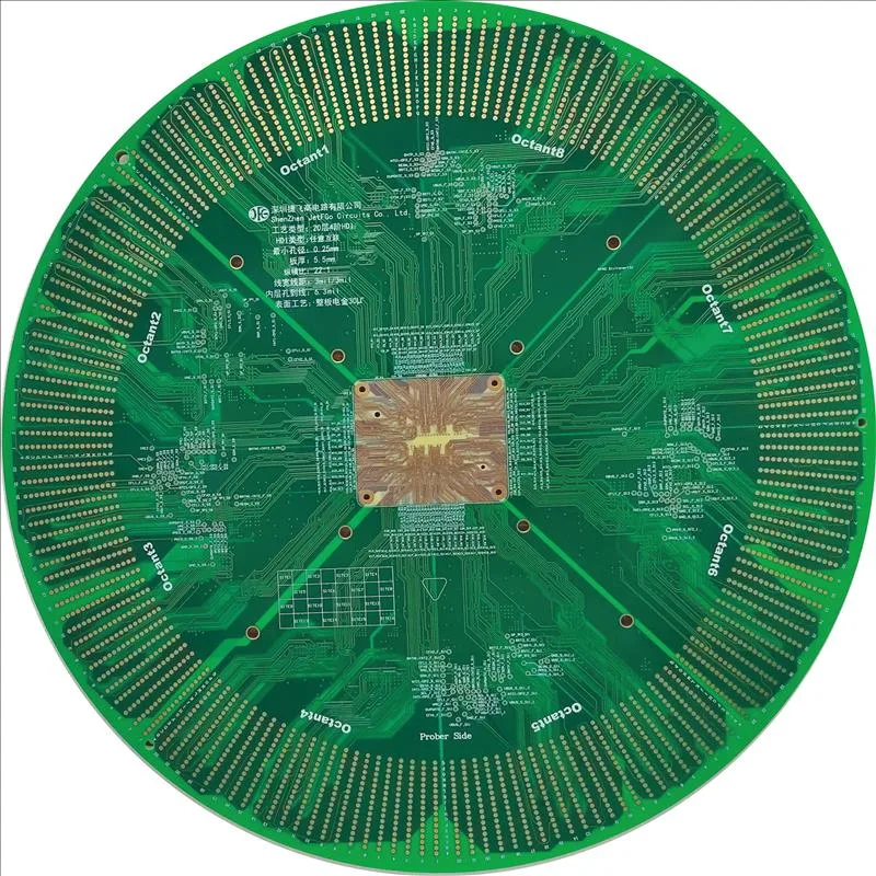
JETFGO / HDI-1N1RIGID
01 / RÉPONSE TECHNIQUE
Réponse technique
02 / DATA
Fenêtre de procédé vérifiée
Parcours HDI pour conceptions compactes, BGA à pas fin et microvias laser.
HDI Build-Up
1+N+1 sequential lamination
Laser Microvia
3–5 mil
BGA Pitch
0.4 mm, subject to fan-out and DFM review
Microvia Structure
Laser-drilled blind microvia
HDI Process
Sequential lamination · laser drilling
Design Review
BGA fan-out · via-in-pad · microvia geometry · stack-up
05 / INPUT
Fichiers pour la revue
HDI Engineering Review Package
Gerber or ODB++, drill files, proposed stack-up, fabrication drawing, quantity, target delivery date and applicable microvia, BGA or via-in-pad requirements.
HDI Stack-up & Via Structure
Provide the proposed 1+N+1 layer structure, microvia layer pairs, dielectric thicknesses and any stacked, staggered or via-in-pad requirements.
BGA Fan-Out Requirements
Provide fine-pitch BGA locations, package pitch, pad geometry and any required via-in-pad or escape-routing constraints that may affect the HDI build-up.
Material & Thickness Requirements
Demander un devisProvide the preferred PCB thickness, copper weight, laminate or Tg requirements and any dielectric constraints relevant to the HDI stack-up.
06 / FAQ
Questions techniques
Les limites publiées proviennent de la matrice de capacités JETFGO. La faisabilité finale exige le dossier complet.
01Is 1+N+1 HDI suitable for every fine-pitch BGA design?+
No. 1+N+1 is a common HDI structure, but final suitability depends on BGA pitch, pad geometry, escape routing, microvia structure, stack-up and required routing density. More complex designs may require additional build-up layers.
02Which files help JETFGO review a 1+N+1 HDI PCB fastest?+
Send Gerber or ODB++, drill files, proposed stack-up, fabrication drawing, quantity, target delivery date and any microvia, BGA fan-out or via-in-pad requirements.
03Can JETFGO support prototypes and repeat production for 1+N+1 HDI PCBs?+
Yes. Once the HDI stack-up, microvia structure, materials and engineering requirements are confirmed, the approved manufacturing data can support prototype validation and repeat production under the same process conditions.
04What does 1+N+1 mean in an HDI PCB stack-up?+
1+N+1 describes an HDI construction with one build-up layer on each side of an N-layer core. Laser-drilled microvias connect the outer build-up layers to adjacent inner layers.
05What is a laser microvia in an HDI PCB?+
A laser microvia is a small laser-drilled interconnect used to connect adjacent PCB layers in an HDI structure. It enables higher routing density than conventional plated through-hole routing.
06Can JETFGO evaluate 0.4 mm BGA designs for 1+N+1 HDI?+
Yes. JETFGO can evaluate 0.4 mm BGA designs, but final feasibility depends on pad geometry, fan-out strategy, microvia size, via-in-pad requirements and the complete PCB stack-up.
07Does 1+N+1 HDI require sequential lamination?+
Yes. A 1+N+1 HDI structure uses build-up layers added around the core, so sequential lamination and laser-drilled microvias are part of the manufacturing process.
RFQ / DFM
Envoyez le besoin. Recevez un plan d’approvisionnement fabricable.
Envoyez Gerber ou ODB++, empilage, matériaux, quantité, date cible et tests pour étude et devis technique.
Revue techniqueMatériaux et empilageFabrication précise