
Ruta térmica y de corriente para conversión de potencia y accionamientos. Ventana de proceso verificada: Copper capability: Rigid inner / outer: 1/3–28 oz; Line / spacing guidance: Copper-dependent process window; IPC class: Class 2 and Class 3 Archivos para revisión: Gerber u ODB++, archivos de taladro, stackup, plano, cantidad y fecha objetivo. Los límites publicados proceden de la tabla actual de capacidades de JETFGO. La viabilidad final requiere el paquete completo.
Los límites publicados proceden de la tabla actual de capacidades de JETFGO. La viabilidad final requiere el paquete completo.Código de soluciónHCP-06OZ+Capacidad verificada
PCB de potencia de cobre pesado
Ruta térmica y de corriente para conversión de potencia y accionamientos.
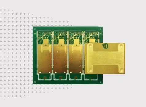
JETFGO / HCP-06OZ+RIGID
01 / RESPUESTA TÉCNICA
Respuesta técnica
02 / DATA
Ventana de proceso verificada
Ruta térmica y de corriente para conversión de potencia y accionamientos.
Copper Weight Capability
Rigid inner / outer: 1/3–28 oz
Line / Spacing Capability
Copper-dependent process window
IPC Workmanship Class
Class 2 and Class 3, subject to project requirements
Power-Path Review
Copper weight · current · trace width · thermal distribution
Heavy-Copper DFM
Stack-up · spacing · vias · copper balance · current paths
Engineering Review
Current · voltage · copper · thermal · mechanical requirements
05 / INPUT
Archivos para revisión
Heavy-Copper Engineering Package
Gerber or ODB++, drill files, proposed stack-up, fabrication drawing, copper-weight requirements, quantity, target delivery date and any current, thermal, spacing or IPC-class requirements.
Copper Weight & Stack-up Requirements
Provide required copper weight by layer, proposed stack-up, board thickness and any heavy-copper areas or layer-specific construction requirements.
Current & Power Requirements
Provide expected current levels, critical power paths, voltage requirements and any defined temperature-rise or thermal-management targets.
Trace & Spacing Requirements
Identify critical trace widths, conductor spacing, high-current nets and any voltage-clearance requirements that may affect the heavy-copper process window.
IPC & Reliability Requirements
Solicitar cotizaciónSpecify the required IPC workmanship class, inspection criteria and any project-specific reliability, qualification or documentation requirements.
06 / FAQ
Preguntas técnicas
Los límites publicados proceden de la tabla actual de capacidades de JETFGO. La viabilidad final requiere el paquete completo.
01What is a heavy-copper PCB?+
A heavy-copper PCB uses increased copper thickness in selected or multiple conductive layers to support higher current, improve thermal distribution and strengthen power paths in demanding electronic systems.
02Which files help JETFGO review a heavy-copper PCB fastest?+
Send Gerber or ODB++, drill files, proposed stack-up, fabrication drawing, required copper weight by layer, quantity, target delivery date and any current, thermal, spacing or IPC-class requirements.
03Can JETFGO support prototypes and repeat production for heavy-copper PCBs?+
Yes. Once the copper weight, stack-up, trace geometry, spacing and manufacturing conditions are confirmed, the approved engineering record can support prototype validation and repeat production.
04Why use heavy copper in a power PCB?+
Heavy copper can support higher-current power paths, improve thermal distribution and provide more robust conductor structures. Final copper weight should be selected together with current, trace geometry, thermal and reliability requirements.
05How does copper weight affect PCB line width and spacing?+
Increasing copper thickness changes the etching and fabrication process window, so achievable line width and spacing depend on the selected copper weight, layer structure and board design.
06Can JETFGO manufacture heavy-copper PCBs up to 28 oz?+
JETFGO’s published rigid-PCB capability range includes inner and outer copper up to 28 oz. Final feasibility depends on the complete stack-up, copper distribution, line and spacing requirements, board size and engineering review.
07Can heavy-copper PCBs be manufactured to IPC Class 3 requirements?+
Heavy-copper projects requiring IPC Class 3 workmanship can be reviewed. Final process controls, inspection criteria and qualification requirements depend on the complete project specification.
08What information is needed to design a high-current PCB?+
Useful information includes operating current, voltage, copper weight, critical trace widths, available board area, expected temperature rise, via current paths, spacing requirements and the proposed PCB stack-up.
09What is the difference between heavy copper PCB and copper inlay PCB?+
A heavy-copper PCB increases copper thickness across selected traces or layers, while a copper-inlay PCB uses localized embedded copper structures to create concentrated thermal or current paths in specific areas.
RFQ / DFM
Envíe el requisito. Reciba un plan de suministro fabricable.
Envíe Gerber u ODB++, stackup, material, cantidad, fecha objetivo y pruebas para revisar la viabilidad y cotizar.
Revisión técnicaMaterial y stackupFabricación precisa