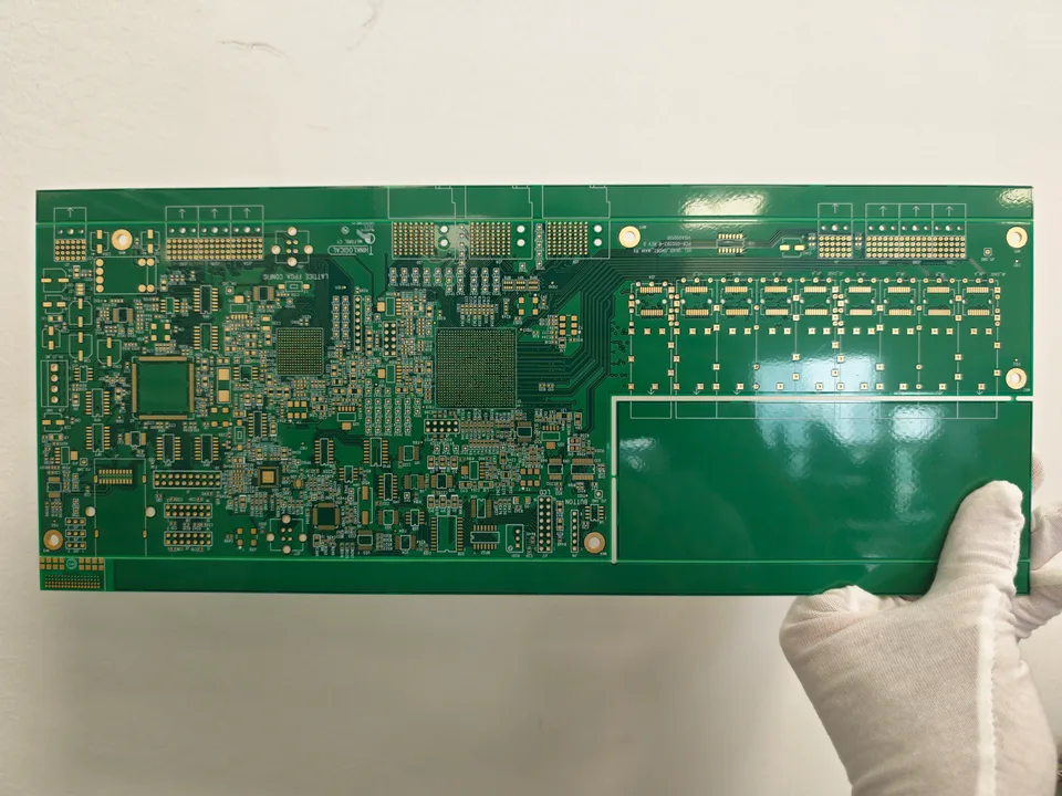
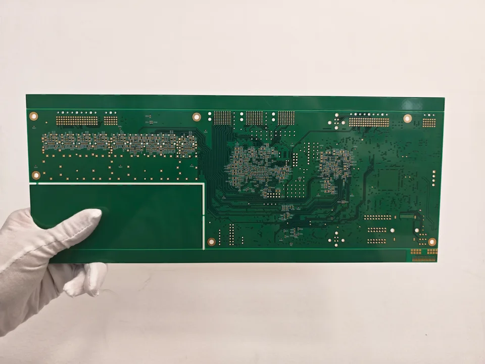
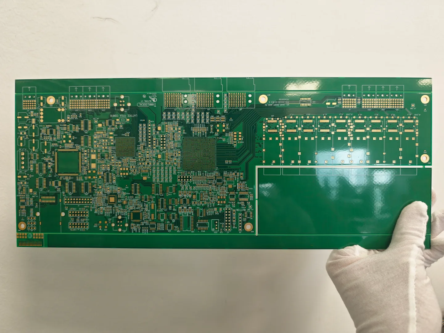
 PRODUCT & PROCESS DETAIL
01 / TECHNICAL PROFILE
Board parameters
- Layer Count
- 12 Layers
- Base Material
- FR-4 (S1000-2M)
- Glass Transition Temperature (Tg)
- 180°C
- Board Thickness
- 1.575 mm
- Inner Layer Trace Width / Spacing
- 5 / 5 mil
- Outer Layer Trace Width / Spacing
- 5 / 5 mil
- Hole-to-Trace Clearance
- 8 mil
- Minimum Hole Diameter
- 0.20 mm
- Inner Copper Weight
- 1 oz
- Outer Copper Weight
- 1 oz
- Copper Stack-up
- 1 oz per layer (12-layer construction)
- Hole Copper Thickness
- 20 μm
- Surface Finish
- ENIG (Electroless Nickel Immersion Gold)
- Gold Thickness
- 2 μin
- Solder Mask
- Double-Sided
- Solder Mask Color
- Green
- Silkscreen Color
- White
- SET Dimensions
- 365.76 × 149.23 mm
- Panelization
- 1 × 1
- Number of Drilled Holes
- 3,292
- Test Points
- 4,850
- Impedance Control
- Yes
- Impedance Control Groups
- 27
- Via Process
- Aluminum Sheet Via Plugging
- Manufacturing Method
- CNC Routing
- Testing Method
- Customer Flying Probe Test
02 / PROJECT RECORD
About this board
Potential Applications and Industry Solutions
This type of multilayer PCB is suitable for industrial automation systems, communication and networking equipment, embedded computing platforms, electronic testing instruments and advanced control systems.
It provides a manufacturing solution for OEM manufacturers, hardware developers and engineering companies working on complex electronic products that require multiple signal layers, controlled impedance and reliable circuit interconnections.
JETFGO supports customized multilayer PCB manufacturing for demanding electronic applications, helping customers move from prototype validation and NPI development to stable volume production.