
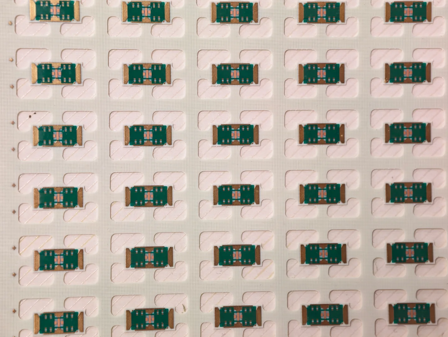
 PRODUCT & PROCESS DETAIL
01 / TECHNICAL PROFILE
Board parameters
- Product Model
- 02N76257A0
- PCB Type
- Thin High-Frequency Laminate PCB
- Layer Count
- 2 Layers
- Base Material
- Rogers RO4350B
- Finished Board Thickness
- 0.30 mm
- Finished Copper Weight
- 1 oz
- Minimum Trace Width
- 4 mil
- Minimum Trace Spacing
- 4.3 mil
- Minimum Hole Diameter
- 0.10 mm
- Hole Aspect Ratio
- 3:1
- Drilling Technology
- Laser Through-Hole Drilling
- Special Hole Process
- Plated-Hole Filling
- Surface Finish
- ENIG + OSP
- Manufacturing Challenge
- Thin-Board Handling and Breakage Prevention
- Fine-Line Process Challenge
- 2.7 mil Spacing After Compensation
- Electroplating Challenge
- Fine-Line Photoresist Pinching Risk
- Key Manufacturing Capability
- Precision Laser Drilling, Hole Plating and Filling
- Production Format
- Multi-Unit Panelization
02 / PROJECT RECORD
About this board
Potential Applications and Industry Solutions
This type of thin Rogers PCB can support RF communication modules, wireless connectivity devices, microwave electronics, compact sensing systems and specialized high-frequency electronic assemblies.
It is particularly relevant to RF equipment manufacturers, wireless technology developers, telecommunications OEMs and engineering teams requiring precision circuit fabrication on thin, high-frequency laminate materials.
JETFGO supports customized high-frequency PCB manufacturing, including precision laser drilling, plated-hole filling, fine-line processing and specialized surface finishing for demanding electronic applications.