 PRODUCT & PROCESS DETAIL
01 / TECHNICAL PROFILE
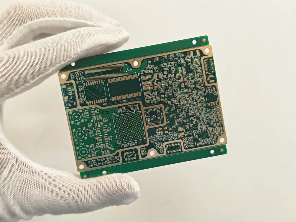
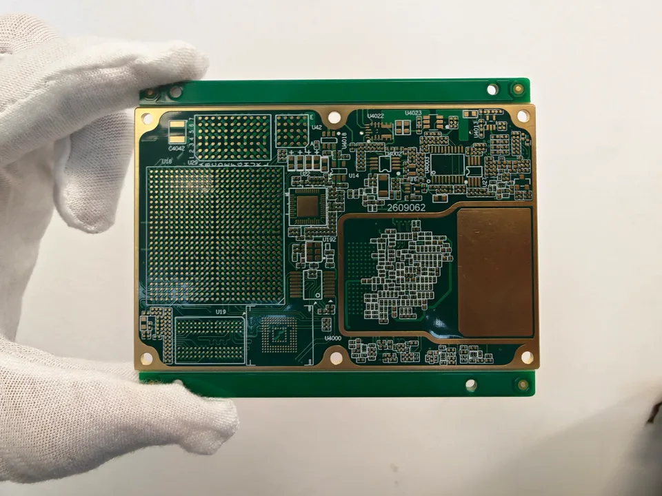
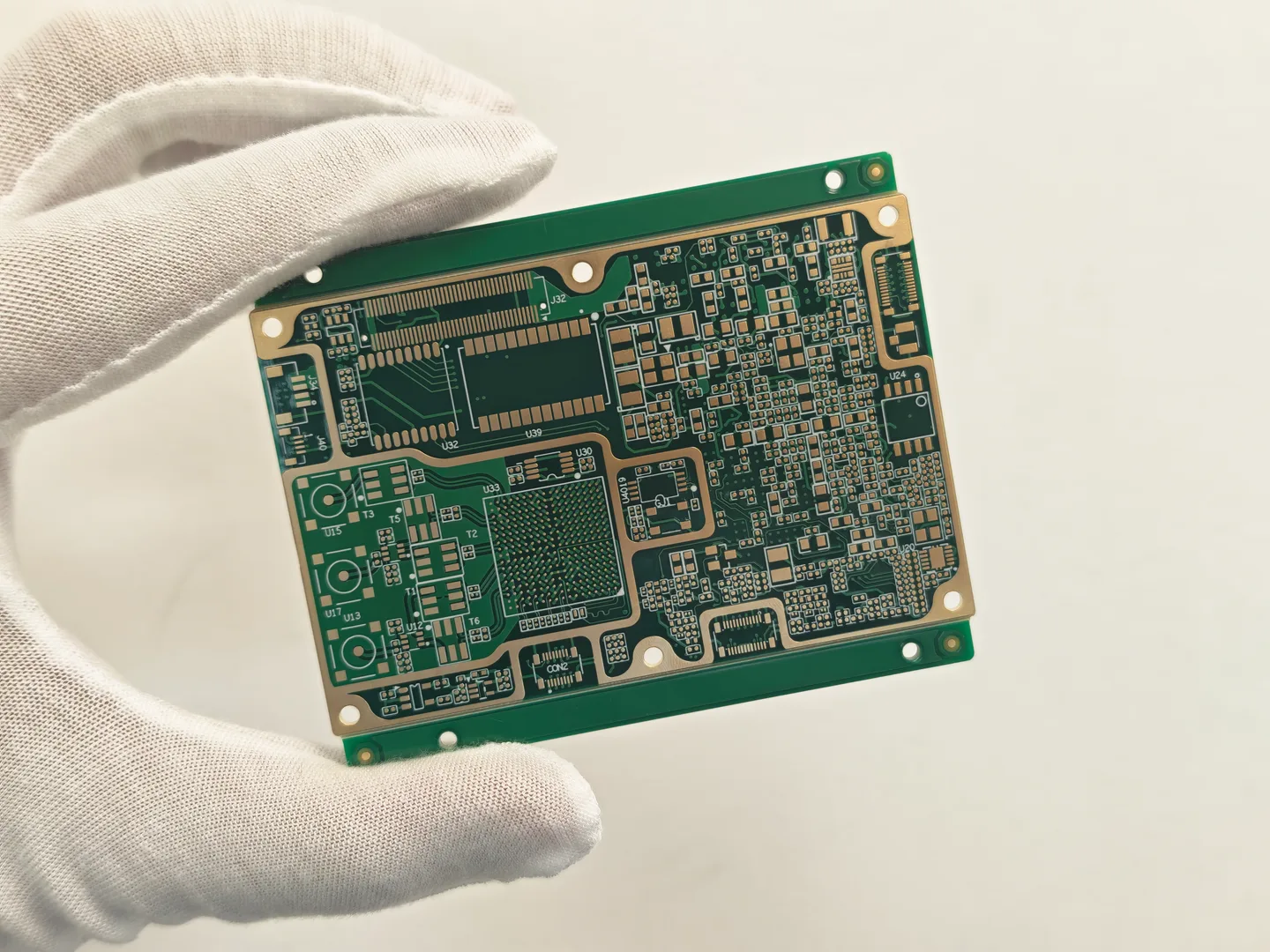
Board parameters
- PCB Type
- High-Density Multilayer PCB
- Layer Count
- 12 Layers
- Base Material
- FR-4 (Shengyi S1000-2M)
- Glass Transition Temperature (Tg)
- 180°C
- Finished Board Thickness
- 1.60 mm
- Inner Layer Trace Width / Spacing
- 4 / 4 mil
- Outer Layer Trace Width / Spacing
- 4 / 4 mil
- Hole-to-Trace Clearance
- 8 mil
- Minimum Hole Diameter
- 0.20 mm
- Inner Layer Copper Weight
- 1 oz
- Outer Layer Copper Weight
- 1 oz
- Copper Stack-up
- 1 oz per Layer
- Plated Hole Copper Thickness
- 18 μm
- Surface Finish
- ENIG (Electroless Nickel Immersion Gold)
- Solder Mask Color
- Green
- Silkscreen Color
- White
- Impedance Control
- Required
- Impedance Control Groups
- 15
- BGA Pad Structure
- High-Density BGA Layout
- SET Dimensions
- 79 × 62.16 mm
- Drilled Hole Count
- 2,295
- Test Points
- 3,631
- Hole Density
- 467,353 Holes/m²
- PCB Profiling
- CNC Routing
- Electrical Testing
- Factory Flying Probe Test
02 / PROJECT RECORD
About this board
Potential Applications and Industry Solutions
This type of high-density multilayer PCB is suitable for embedded computing systems, industrial automation controllers, communication equipment, precision electronic instruments and advanced signal-processing modules.
It is particularly relevant to electronics OEMs, embedded hardware developers, industrial equipment manufacturers and engineering teams requiring compact circuit integration, high-density BGA connections and controlled signal transmission.
JETFGO provides customized multilayer PCB manufacturing solutions, supporting complex electronic projects from prototype validation and NPI to volume production.