
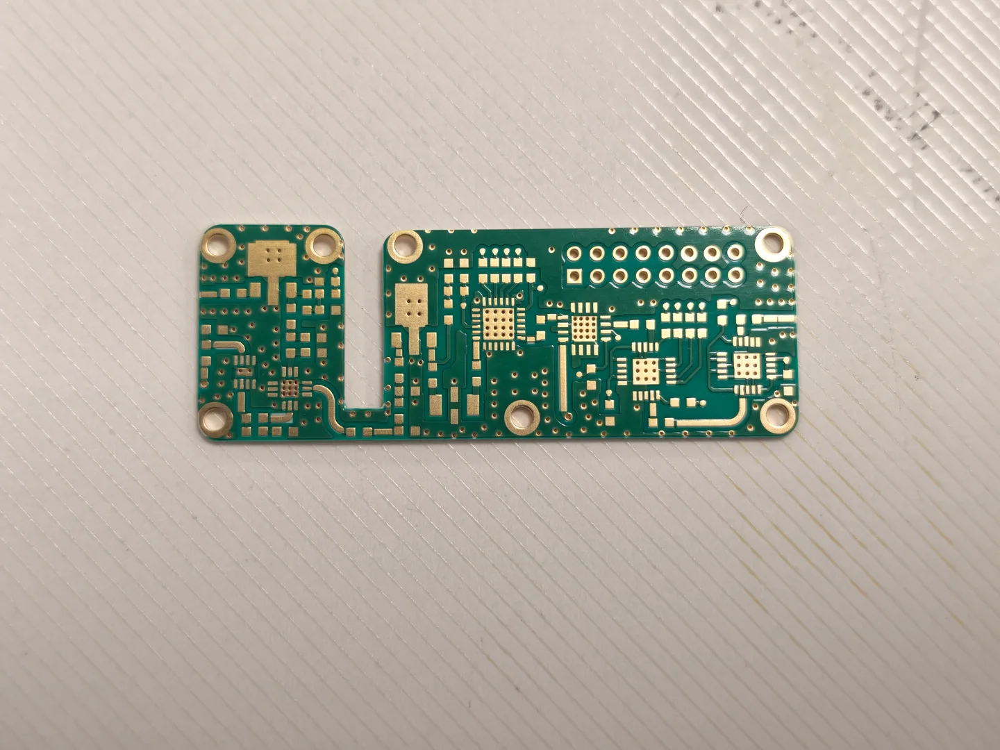
 PRODUCT & PROCESS DETAIL
Board parameters
- Product Model
- 04C76237
- PCB Type
- Hybrid High-Frequency HDI PCB
- Layer Count
- 4 Layers
- Base Materials
- R4350B + S1000H
- High-Frequency Material
- Rogers RO4350B
- Additional Laminate
- S1000H
- Laminate Construction
- Hybrid-Material Lamination
- Finished Board Thickness
- 0.80 mm
- Finished Copper Weight
- 1 oz per Layer
- Copper Stack-up
- 1/1/1/1 oz
- Minimum Trace Width
- 8 mil
- Minimum Trace Spacing
- 8 mil
- Minimum Hole Diameter
- 0.15 mm
- Hole Aspect Ratio
- 5:1 (Process Card Specification)
- Surface Finish
- Immersion Gold
- Special Technology
- HDI + High Frequency + Hybrid Lamination
- Visible Board Features
- Irregular Profile, Mounting Holes, Dense Component Pads and Plated Connections
- Solder Mask Color
- Green
- Silkscreen Color
- White
- Key Manufacturing Processes
- Hybrid Lamination, HDI Fabrication, Precision Hole Processing and Surface Finishing
- Primary Manufacturing Challenges
- Material Compatibility, Thin-Board Handling, Hole Formation Accuracy and Multilayer Registration
About this board
Potential Applications and Industry Solutions
Hybrid high-frequency PCBs can be used in RF communication modules, wireless networking equipment, signal-processing circuits, telecommunications devices, industrial sensing systems and specialized electronic test instruments.
This type of PCB is particularly relevant to RF equipment manufacturers, wireless technology developers, telecommunications OEMs and engineering teams developing compact electronic systems that require specialized laminate materials and precise circuit interconnections.
JETFGO supports customized RF and HDI PCB manufacturing, including hybrid-material lamination, precision hole processing and complex board profiling, helping customers meet manufacturing requirements from prototype validation to volume production.