
 PRODUCT & PROCESS DETAIL
01 / TECHNICAL PROFILE
Board parameters
- Product Model
- 06H76466C0
- PCB Type
- High-Frequency Stepped Multilayer PCB
- Layer Count
- 6 Layers
- Base Material
- Rogers 4350B
- Finished Board Thickness
- 1.18 mm
- Inner Layer Copper Weight
- 0.5 oz
- Outer Layer Copper Weight
- 1 oz
- Minimum Trace Width
- 11.3 mil
- Minimum Trace Spacing
- 3.2 mil
- Minimum Hole Diameter
- 0.25 mm
- Hole Aspect Ratio
- 4.32:1 (Process Card Specification)
- Surface Finish
- NiPdAu (Nickel-Palladium-Gold)
- Application Area
- 5G Communication
- Special Manufacturing Process
- Two-Level Stepped Structure
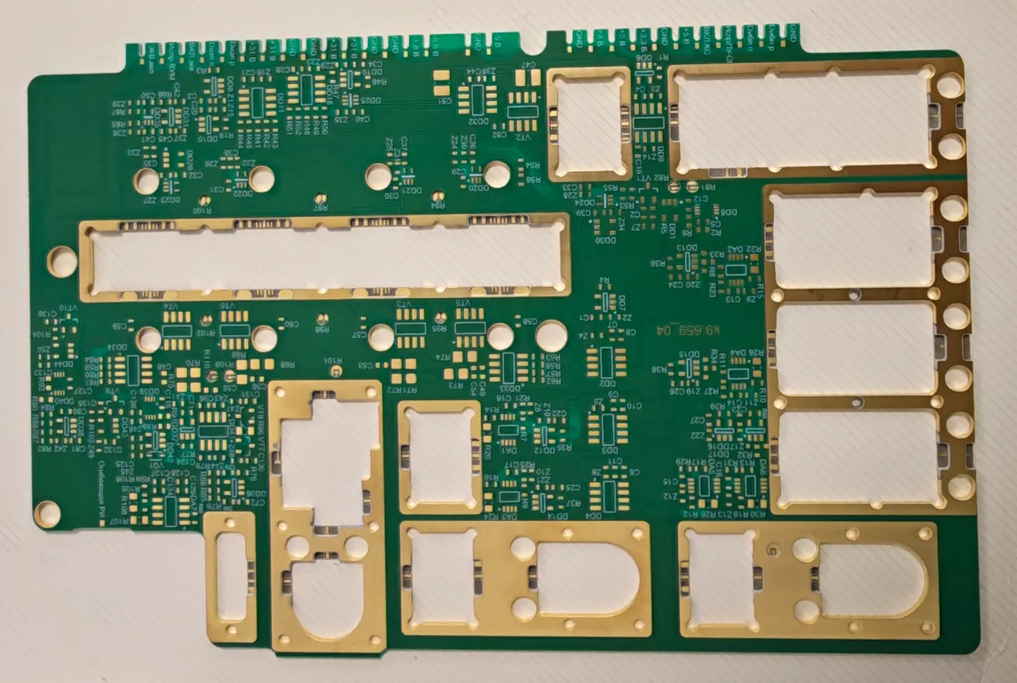
- Visible Board Features
- Large Custom Cutouts, Non-Standard Board Profile and Multiple Connection Pads
- Solder Mask Color
- Green
- Key Manufacturing Processes
- Rogers High-Frequency Laminate Processing, Stepped Structure Fabrication, Precision Drilling and Custom PCB Profiling
- Primary Manufacturing Challenges
- Stepped Structure Dimensional Control, High-Frequency Material Processing, Narrow Trace Spacing and Complex Cutout Accuracy
02 / PROJECT RECORD
About this board
A specialized multilayer circuit board featuring complex mechanical openings, precision connection areas and customized structural processing. Its combination of high-frequency laminate fabrication, intricate PCB profiling and selective surface finishing demonstrates JETFGO's ability to manufacture demanding RF circuit designs.