
 PRODUCT & PROCESS DETAIL
Board parameters
- Product Model
- 10C85585A0
- PCB Type
- Heavy Copper HDI Power Control PCB
- Layer Count
- 10 Layers
- Base Material
- Shengyi S1000-2M
- Finished Board Thickness
- 2.60 mm
- Inner Layer Finished Copper Weight
- 3 oz
- Outer Layer Finished Copper Weight
- 2 oz
- Copper Configuration
- 3 oz Inner Layers / 2 oz Outer Layers
- Minimum Trace Width
- 12.8 mil
- Minimum Trace Spacing
- 7.4 mil
- Minimum Hole Diameter
- 0.35 mm
- Hole Aspect Ratio
- 7.43:1
- Surface Finish
- ENIG (Electroless Nickel Immersion Gold)
- Application Area
- Power Control
- HDI Technology
- First-Order HDI
- Special Via Technology
- Buried Vias
- Special Manufacturing Process
- Heavy Copper Fabrication
- Solder Mask Color
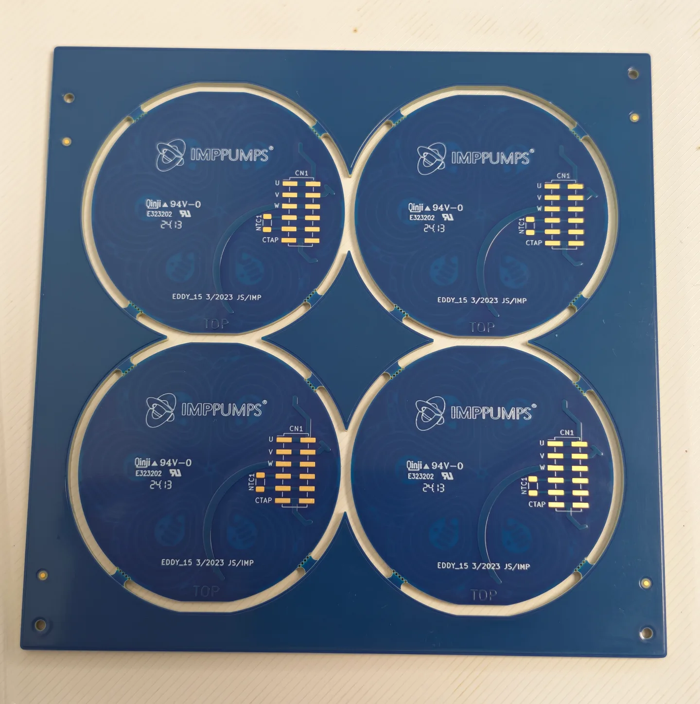
- Blue
- Silkscreen Color
- White
- Visible Board Structure
- Four Circular PCB Units in a Panel
- Visible Electrical Markings
- U, V, W, NTC1 and CTAP
- Key Manufacturing Processes
- Heavy Copper Etching, First-Order HDI Fabrication, Buried Via Processing, Multilayer Lamination and Precision Drilling
- Primary Manufacturing Challenges
- Heavy Copper Etching Control, Multilayer Registration, Buried Via Interconnections, Lamination Reliability and Hole Metallization
About this board
Potential Applications and Industry Solutions
This type of heavy copper HDI PCB is suitable for industrial power control equipment, electric motor controllers, pump drive systems, power conversion modules, industrial automation equipment and specialized power electronics.
It is particularly relevant to industrial equipment manufacturers, motor drive developers, pump system OEMs and power electronics engineering teams requiring multilayer circuit integration, substantial copper thickness and complex internal interconnections.
JETFGO supports customized heavy copper and HDI PCB manufacturing, including thick-copper processing, buried via fabrication and multilayer lamination, helping customers move from prototype validation and NPI to volume production.