
 PRODUCT & PROCESS DETAIL
Board parameters
- Product Model
- 04H84792A0
- PCB Type
- RF PCB with Copper Inlay and Reinforcement
- Layer Count
- 4 Layers
- Base Material
- Panasonic M6
- Finished Board Thickness
- 1.90 mm
- Inner Layer Finished Copper Weight
- 0.5 oz
- Outer Layer Finished Copper Weight
- 1 oz
- Copper Configuration
- 0.5 oz Inner / 1 oz Outer
- Trace Width
- 19 mil
- Trace Spacing
- 5.5 mil
- Minimum Hole Diameter
- 0.25 mm
- Hole Aspect Ratio
- 2.8:1 (Process Card Value; Verification Required)
- Surface Finish
- NiPdAu (Nickel-Palladium-Gold)
- Special Manufacturing Process
- Copper Inlay
- Mechanical Reinforcement
- Copper Plate Reinforcement
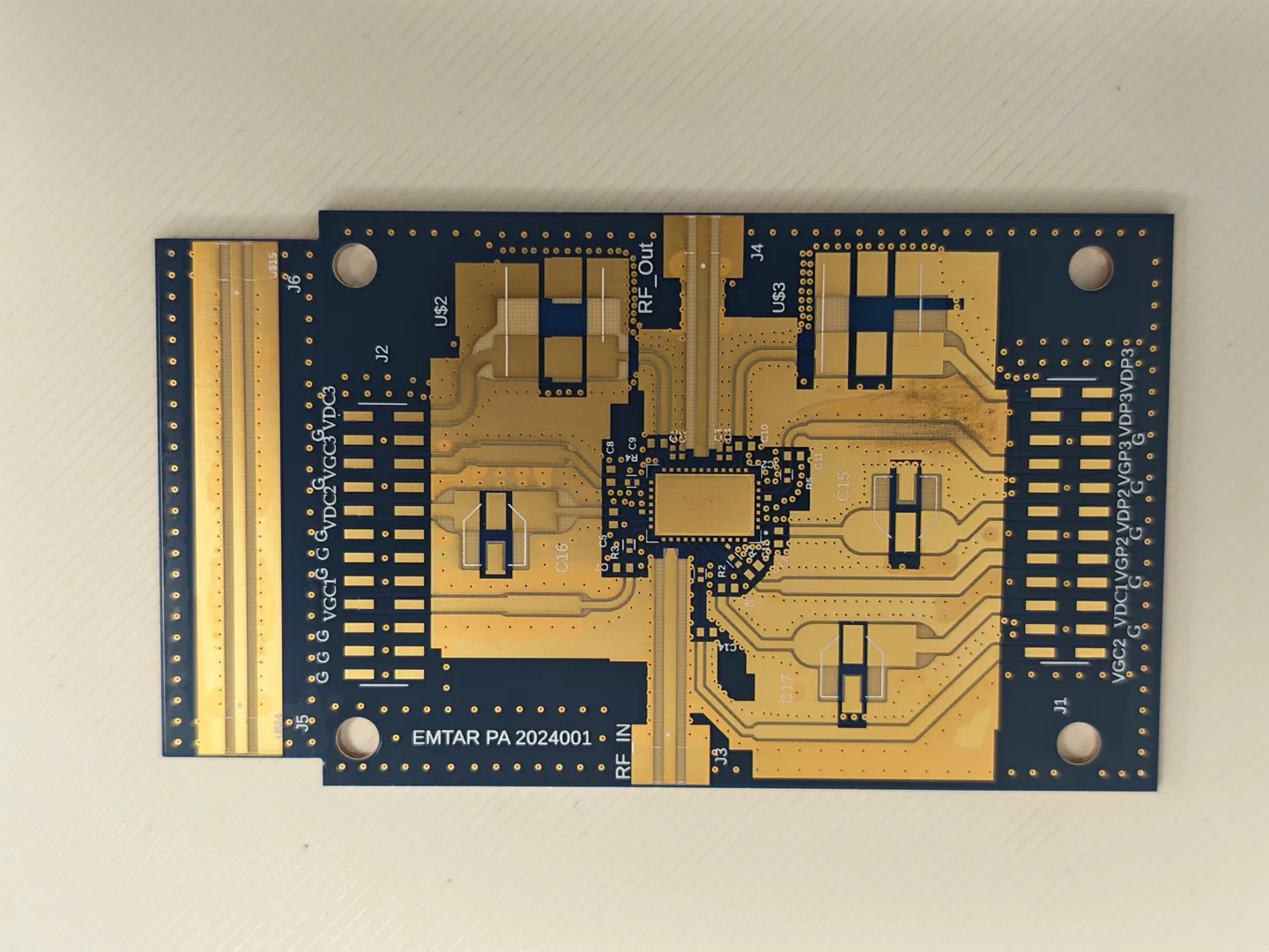
- Visible RF Connections
- RF_IN and RF_OUT
- Visible Board Marking
- EMTAR PA 2024001
- Visible Circuit Features
- RF Signal Routing, Wide Copper Areas, Multiple Connection Pads and Mounting Holes
- Solder Mask Color
- Dark Blue
- Silkscreen Color
- White
- Key Manufacturing Processes
- Panasonic M6 Laminate Processing, Copper Inlay Integration, Copper Reinforcement, Precision Circuit Etching and NiPdAu Finishing
- Primary Manufacturing Challenges
- Embedded Copper Integration, Lamination Compatibility, Reinforcement Alignment, Circuit Dimensional Control and Surface Finish Consistency
About this board
Potential Applications and Industry Solutions
This type of specialized RF PCB is suitable for RF amplifier modules, wireless communication equipment, aerospace communication electronics, RF signal-processing systems and high-performance electronic test instruments.
It is particularly relevant to RF hardware developers, telecommunications equipment manufacturers, aerospace electronics OEMs and engineering teams requiring specialized laminate materials, integrated copper structures and precision signal interconnections.
JETFGO supports customized RF and high-speed PCB manufacturing, including copper inlay processing, copper plate reinforcement, precision circuit fabrication and specialized surface finishing, helping customers move from prototype validation and NPI to volume production.