
 PRODUCT & PROCESS DETAIL
01 / TECHNICAL PROFILE
Board parameters
- Material Type
- Copper-Clad Laminate (CCL)
- Base Material Options
- FR-4, High-Tg FR-4, Halogen-Free Laminates
- FR-4 Material Grades
- Tg135, Tg150, Tg170, Tg180
- Material Suppliers
- Shengyi, ITEQ, KB, EMC
- Rigid PCB Layer Count
- Up to 60 Layers
- Rigid PCB Thickness Range
- 0.3–8.0 mm
- Inner-Layer Copper Weight
- 1/3–28 oz
- Outer-Layer Copper Weight
- 1/3–28 oz
- Minimum Trace Width / Spacing
- 3 / 2.5 mil
- Minimum Finished PCB Size
- 10 × 10 mm
- Controlled Impedance Tolerance
- ±8%
- Mechanical Drilling Aspect Ratio
- Up to 20:1
- Laser-Drilled Microvia Diameter
- 3–5 mil
- Available Surface Finishes
- HASL, Lead-Free HASL, OSP, ENIG, ENEPIG, Immersion Silver, Immersion Tin, Gold Plating
- Solder Mask Options
- Green, Black, White, Blue, Red, Yellow, Purple, Gray
- Manufacturing Services
- PCB Prototyping, Multilayer Fabrication, Small-Batch and Volume Production
- Engineering Review
- Material Availability, Copper Thickness, Stackup and Process Feasibility Subject to Confirmation
02 / PROJECT RECORD
About this board
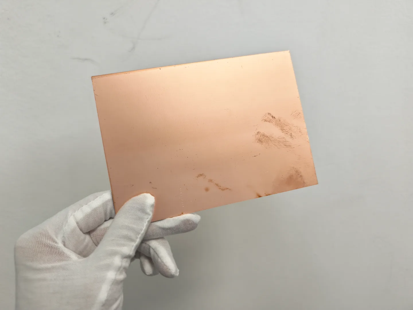
Standard Copper-Clad PCB Base Material
Manufactured using copper foil bonded to an insulating laminate substrate, providing the foundation for PCB circuit fabrication. Material selection focuses on copper adhesion, electrical insulation, dimensional stability and thermal reliability.
JETFGO supports FR-4, high-Tg and other specialized PCB laminate materials, with substrate thickness and copper weight selected according to customer specifications and manufacturing requirements.