
 PRODUCT & PROCESS DETAIL
01 / TECHNICAL PROFILE
Board parameters
- Layer Count
- 4 Layers
- Base Material
- FR-4 (Kingboard KB-6164)
- Glass Transition Temperature (Tg)
- 140°C
- Board Thickness
- 1.0 mm
- Board Thickness Tolerance
- ±0.1 mm
- Inner Layer Trace Width / Spacing
- 8 / 8 mil
- Outer Layer Trace Width / Spacing
- 8 / 8 mil
- Hole-to-Trace Clearance
- 8 mil
- Minimum Hole Diameter
- 0.25 mm
- Inner Copper Weight
- 1 oz
- Outer Copper Weight
- 1 oz
- Copper Stack-up
- 1 / 1 / 1 / 1 oz
- Hole Copper Thickness
- 20 μm
- Surface Finish
- ENIG (Electroless Nickel Immersion Gold)
- Solder Mask
- Double-Sided
- Solder Mask Color
- White
- Silkscreen
- None
- PCB Dimensions
- 230 × 230 mm
- Production Set Dimensions
- 250 × 250 mm
- Number of Drilled Holes
- 930
- Test Points
- 1,404
- Routing Method
- CNC Routing
- Via Process
- According to Design Files
02 / PROJECT RECORD
About this board
Potential Applications and Industry Solutions
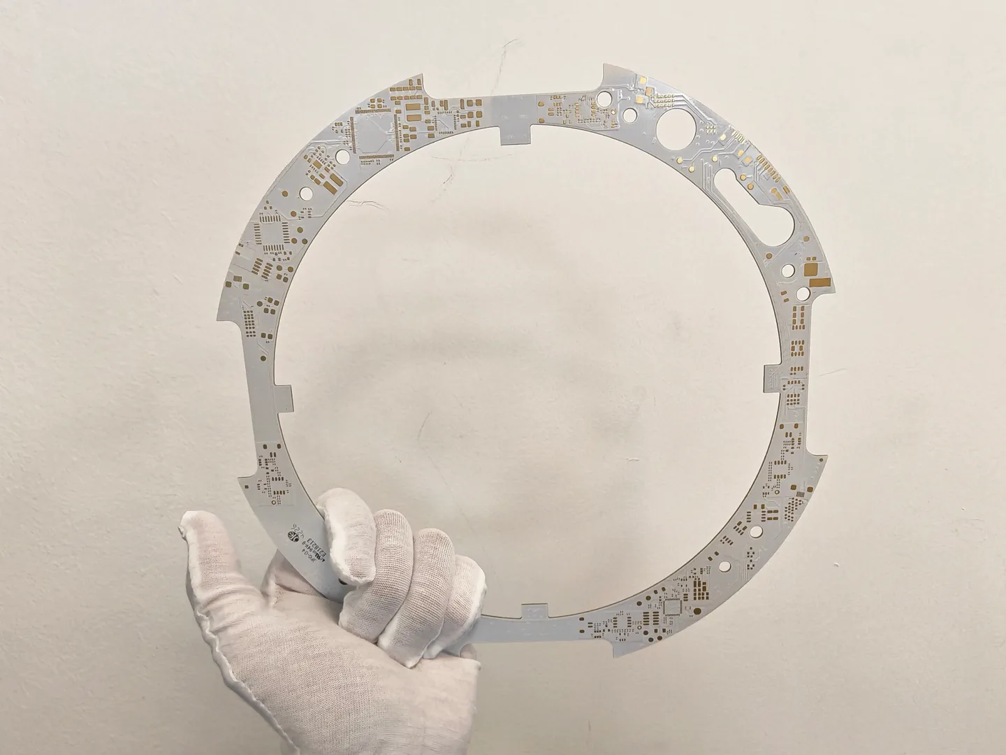
Ring-shaped PCBs can be used in industrial vision systems, optical inspection equipment, circular lighting modules, sensor assemblies and specialized electronic instruments.
They are particularly suitable for manufacturers developing customized industrial equipment, optical devices, smart hardware and electronic systems requiring non-standard PCB geometries.
JETFGO supports customized PCB fabrication, including special-shaped routing, multilayer construction and application-specific manufacturing requirements, from prototype development to volume production.