
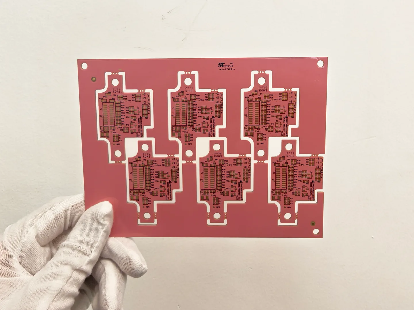
 PRODUCT & PROCESS DETAIL
Board parameters
- Layer Count
- 4 Layers
- Base Material
- FR-4 (KB-6167F)
- Glass Transition Temperature (Tg)
- 170°C
- Board Thickness
- 1.575 mm
- Inner Layer Trace Width / Spacing
- 8 / 8 mil
- Outer Layer Trace Width / Spacing
- 8 / 8 mil
- Hole-to-Trace Clearance
- 8 mil
- Minimum Hole Diameter
- 0.20 mm
- Inner Copper Weight
- 1 oz
- Outer Copper Weight
- 1 oz
- Copper Stack-up
- 1/1/1/1 oz
- Hole Copper Thickness
- 20 μm
- Surface Finish
- ENIG (Electroless Nickel Immersion Gold)
- Gold Thickness
- 2 μin
- Nickel Thickness
- 120 μin
- Solder Mask Color
- Pink
- Silkscreen Color
- Black
- Silkscreen Ink Model
- Guangxin KSM-388BK+
- Panelization
- 3 × 2 (6 Units per Panel)
- Panel Dimensions
- 146.35 × 110.06 mm
- Panel Hole Count
- 1,100
- Total Hole Count
- 1,466
- Hole Density
- 68,293 holes/m²
- Via Process
- According to Design Files
- Manufacturing Method
- CNC Routing
- Testing Method
- Factory Flying Probe Test
About this board
Application Areas and Engineering Solutions
This PCB can be used in industrial electronics, embedded control systems, electronic instrumentation, consumer electronics and customized electronic modules.
It is suitable for OEM/ODM manufacturers, hardware developers and electronic product engineering teams requiring reliable multilayer circuit boards for compact electronic systems, control modules and integrated circuit applications.
The 3 × 2 panelized structure supports the manufacturing of multiple identical PCB units in one panel, making it suitable for prototype development, assembly validation and subsequent production.
JETFGO provides customized PCB manufacturing solutions to support different engineering requirements and production stages.