
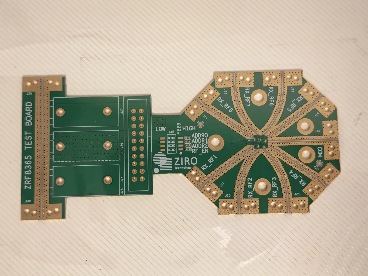
 PRODUCT & PROCESS DETAIL
Board parameters
- Product Model
- 04C73460A0
- PCB Type
- Hybrid-Material RF PCB
- Layer Count
- 4 Layers
- Base Materials
- Taconic TSM-DS3 + S1000-2M
- Laminate Construction
- Mixed-Dielectric Hybrid Lamination
- Finished Board Thickness
- 1.60 mm
- Inner Layer Copper Weight
- 1 oz
- Outer Layer Copper Weight
- 1.5 oz
- Minimum Trace Width
- 4 mil
- Minimum Trace Spacing
- 5.5 mil
- Minimum Hole Diameter
- 0.175 mm
- Hole Aspect Ratio
- 9.14:1
- BGA Feature Size
- 0.18 mm
- Surface Finish
- Immersion Gold
- Via Filling Process
- Resin Plugging
- Edge Treatment
- Metal Edge Plating
- Signal Trace Tolerance
- ±15 μm
- BGA Feature Tolerance
- ±10%
- Surface Copper Tolerance
- ±5 μm
- Key Manufacturing Processes
- Hybrid Lamination, Fine-Line Etching, Resin Via Plugging, Edge Metallization
- Primary Technical Challenges
- Material Compatibility, Precise RF Trace Dimensions, Copper Thickness Control and Fine-Pitch Processing
About this board
Potential Applications and Industry Solutions
This type of RF PCB can be used in radio-frequency test systems, RF switching and signal distribution modules, wireless communication equipment, laboratory measurement instruments and specialized RF evaluation platforms.
It is particularly relevant to RF engineering companies, telecommunications equipment manufacturers, wireless technology developers and electronic test equipment OEMs requiring precise RF signal routing and reliable circuit interconnections.
JETFGO supports hybrid-material PCB manufacturing for specialized RF applications, including mixed-dielectric lamination, precision circuit fabrication, resin-plugged vias and metal edge plating. Our manufacturing services help engineering teams move from prototype verification to production.