
 PRODUCT & PROCESS DETAIL
01 / TECHNICAL PROFILE
Board parameters
- Product Model
- 02D76828A0
- PCB Type
- Nickel-Free Soft Gold PCB
- Layer Count
- 2 Layers
- Base Material
- KB-61610
- Finished Board Thickness
- 1.20 mm
- Finished Copper Weight
- 1 oz
- Minimum Hole Diameter
- 0.20 mm
- Hole Aspect Ratio
- 6:1
- Surface Finish
- Electroplated Gold
- Special Gold Plating Process
- Soft Gold Electroplating
- Nickel-Free Plating
- Yes
- Gold Plating Coverage
- Full-Board Nickel-Free Electrogold Process
- Single-Side Lateral Etching Limit
- ≤25 μm
- Solder Mask Color
- Green
- Contact Pad Structure
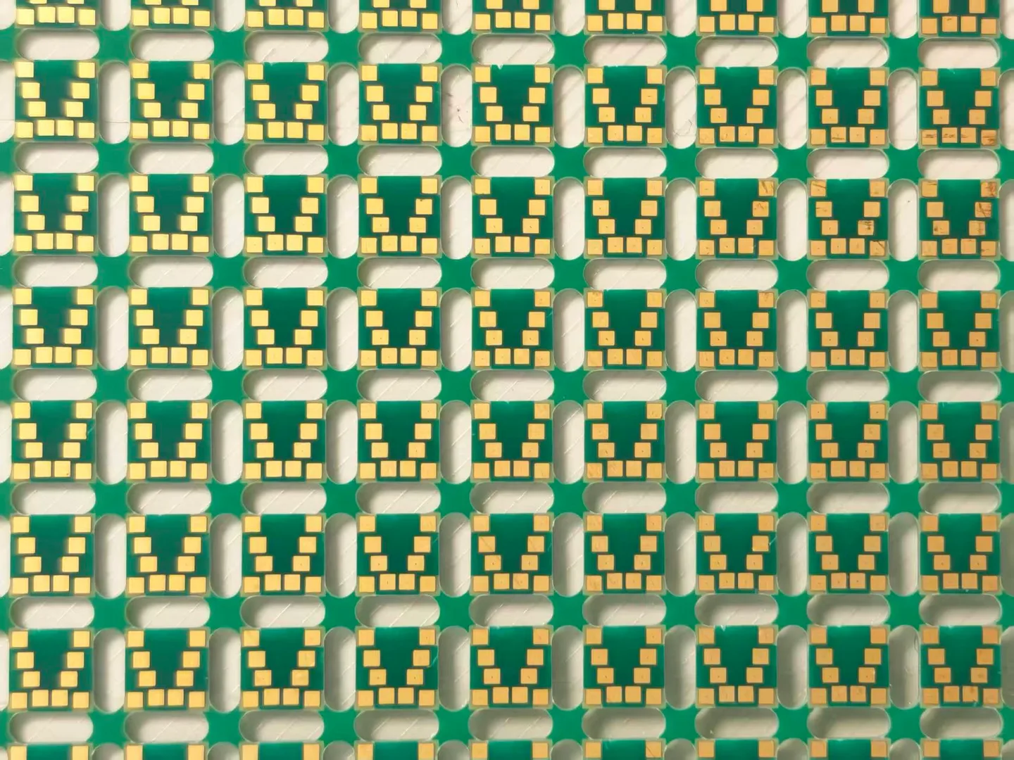
- Repeated Miniature Gold-Plated Pads
- Production Format
- Multi-Unit PCB Panelization
- Key Manufacturing Processes
- Nickel-Free Gold Electroplating, Soft Gold Finishing, Precision Copper Etching
- Primary Manufacturing Challenges
- Nickel-Free Gold Plating and Lateral Etching Control
02 / PROJECT RECORD
About this board
Potential Applications and Industry Solutions
This type of PCB can be considered for electronic testing fixtures, precision contact modules, semiconductor test interfaces, miniature sensor assemblies and specialized electronic interconnection systems.
It is particularly relevant to electronic test equipment manufacturers, semiconductor equipment developers, sensor manufacturers and OEM engineering teams requiring customized gold-plated contact surfaces.
JETFGO supports specialized PCB manufacturing processes, including nickel-free soft gold electroplating, precision copper etching and multi-unit PCB fabrication for demanding contact and interconnection applications.