
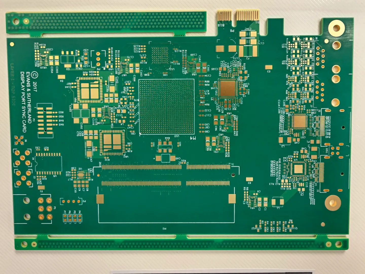
 PRODUCT & PROCESS DETAIL
Board parameters
- Product Model
- 12U52671
- PCB Type
- Precision Gold Finger Multilayer PCB
- Layer Count
- 12 Layers
- Base Material
- FR-4 (S1000-2M)
- Finished Board Thickness
- 1.57 mm
- Outer Layer Copper Weight
- 1 oz
- Inner Layer Copper Weight
- H (Engineering Stack-up Designation)
- Copper Stack-up
- 1/H/H/H/H/H/H/H/H/H/H/1
- Minimum Trace Width
- 4 mil
- Minimum Trace Spacing
- 4 mil
- Minimum Hole Diameter
- 0.20 mm
- Hole Aspect Ratio
- 8:1
- Surface Finish
- Immersion Gold + Electroplated Gold
- Special Plating Process
- Selective Gold Electroplating
- Gold Finger Configuration
- Long and Short Gold Fingers
- Gold Finger Plating Specification
- 51U (As Specified on Process Card)
- Solder Mask Color
- Green
- Silkscreen Color
- White
- Connector Structure
- PCB Edge Contacts
- Visible Board Identification
- Display Port Sync Card
- Key Manufacturing Processes
- Multilayer Lamination, Fine-Line Etching, Selective Gold Plating, Precision Gold Finger Fabrication
- Primary Manufacturing Challenges
- Multilayer Registration, Fine-Line Control, Gold Finger Dimensional Accuracy and Consistent Plating Quality
About this board
Potential Applications and Industry Solutions
This type of multilayer PCB is suitable for professional display systems, graphics interface modules, display synchronization equipment, industrial computing platforms, electronic test instruments and specialized communication interfaces.
It is particularly relevant to professional visualization equipment manufacturers, industrial computer OEMs, embedded hardware developers and engineering teams requiring compact multilayer circuit integration and precision board-to-board connections.
JETFGO provides customized multilayer PCB manufacturing solutions, including fine-line fabrication, selective gold plating, long and short gold finger processing and precision dimensional control, supporting customers from prototype verification to NPI and volume production.