 PRODUCT & PROCESS DETAIL
Board parameters
- Product Model
- 10U76570
- PCB Type
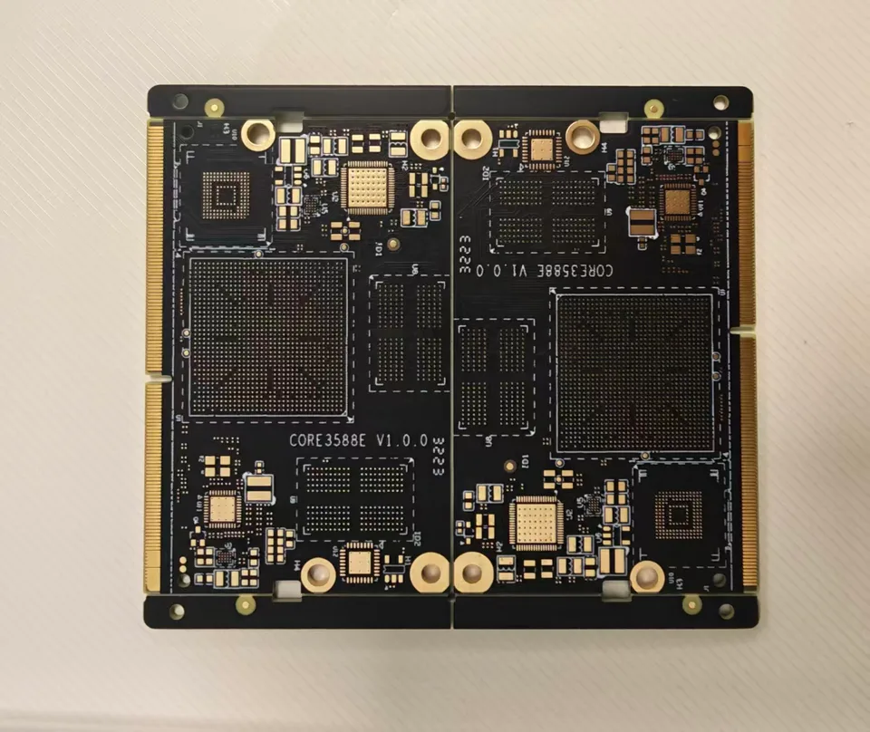
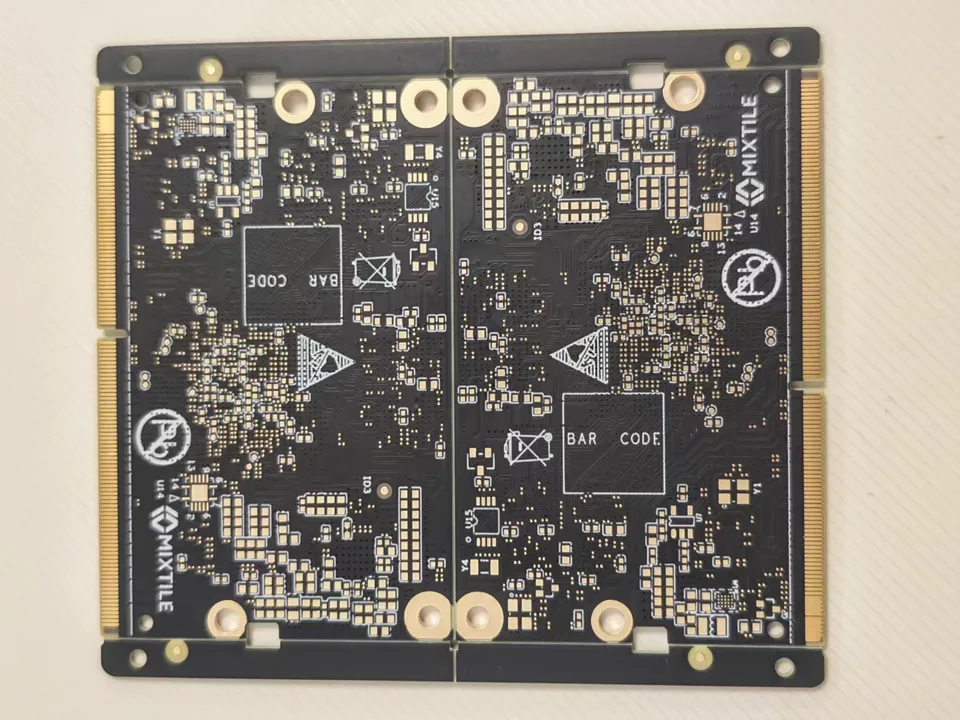
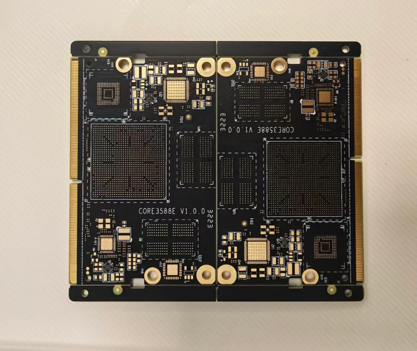
- High-Density Multilayer Gold Finger PCB
- Layer Count
- 10 Layers
- Base Material
- FR-4 (S1000-2M)
- Finished Board Thickness
- 1.20 mm
- Finished Copper Weight
- 1 oz per Layer
- Copper Stack-up
- 1/1/1/1/1/1/1/1/1/1
- Minimum Trace Width
- 3.2 mil
- Minimum Trace Spacing
- 3.2 mil
- Minimum Hole Diameter
- 0.20 mm
- Hole Aspect Ratio
- 6:1
- Surface Finish
- Immersion Gold + Electroplated Gold
- Gold Finger Process
- Selective Gold Plating
- Connector Structure
- PCB Edge Gold Fingers
- BGA Layout
- High-Density BGA Component Footprints
- Impedance Control
- Required
- Impedance Control Groups
- 30
- Solder Mask Color
- Black
- Silkscreen Color
- White
- Visible Board Marking
- CORE3588E V1.0.0
- Visible Brand Marking
- MIXTILE
- Key Manufacturing Processes
- Fine-Line Etching, Multilayer Lamination, Controlled-Impedance Fabrication, Gold Finger Plating
- Primary Manufacturing Challenges
- Fine-Line Dimensional Control, Multilayer Registration, Dense BGA Routing and Multiple Impedance Requirements
About this board
Potential Applications and Industry Solutions
This type of high-density PCB is suitable for embedded computing modules, edge AI devices, industrial computers, intelligent vision systems, robotics controllers and high-performance electronic processing platforms.
It is particularly relevant to embedded system manufacturers, industrial computing OEMs, AI hardware developers and engineering teams developing compact processor modules that require high-density BGA connections, controlled signal routing and reliable board-to-board interfaces.
JETFGO supports customized multilayer PCB manufacturing for these applications, including fine-line fabrication, controlled-impedance processing, precision gold finger manufacturing and high-density circuit integration, from prototype validation and NPI to volume production.