 PRODUCT & PROCESS DETAIL
Board parameters
- Product Model
- 12B71099
- PCB Type
- Heavy Copper Multilayer PCB
- Layer Count
- 12 Layers
- Base Material
- ITEQ IT180
- Finished Board Thickness
- 2.70 mm
- Outer Layer Finished Copper Weight
- 3.5 oz
- Inner Layer Finished Copper Weight
- 3 oz
- Copper Stack-up
- 3.5 oz Outer Layers / 3 oz Inner Layers
- Minimum Trace Width
- 20 mil
- Minimum Trace Spacing
- 20 mil
- Minimum Hole Diameter
- 0.35 mm
- Hole Aspect Ratio
- 8:1
- Surface Finish
- Lead-Free HASL
- Special Manufacturing Process
- Heavy Copper PCB Fabrication
- Solder Mask Color
- Green
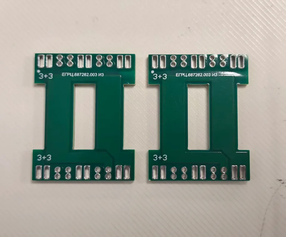
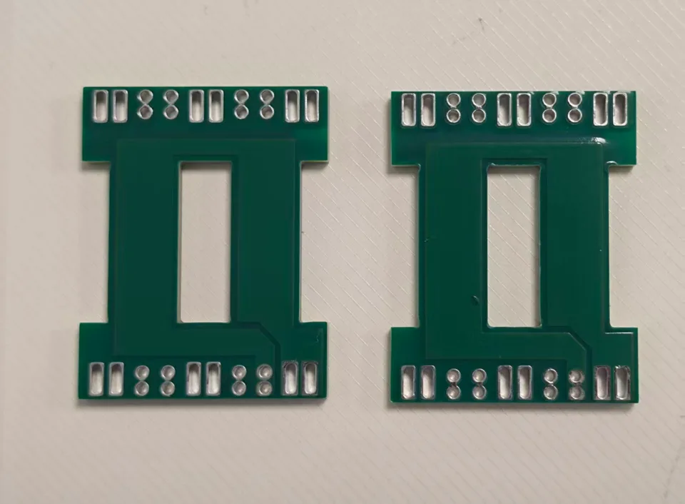
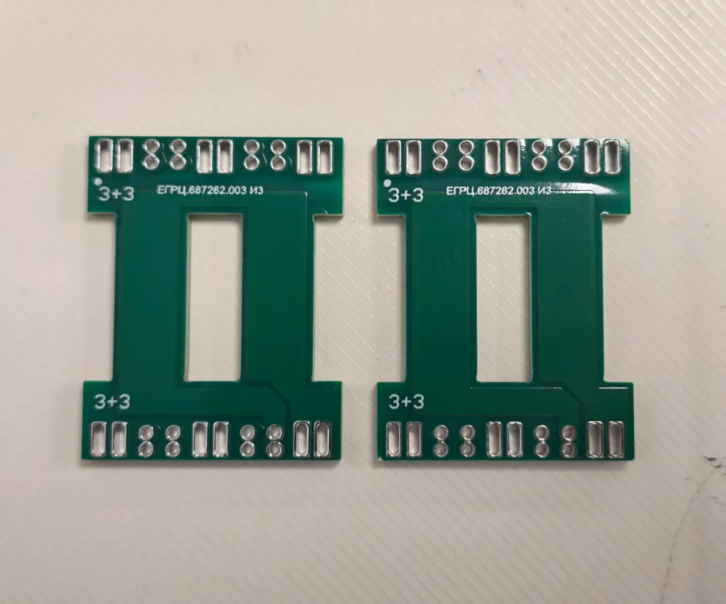
- Board Geometry
- Custom-Shaped PCB with Rectangular Cutouts
- Visible Connection Features
- Plated Through-Hole Pads and Slotted Openings
- Key Manufacturing Processes
- Heavy Copper Etching, Multilayer Lamination, Precision Drilling, CNC Profiling
- Primary Manufacturing Challenges
- Thick-Copper Etching Control, Interlayer Registration, Multilayer Lamination and Dimensional Accuracy
About this board
Potential Applications and Industry Solutions
Heavy copper multilayer PCBs can be used in industrial power distribution systems, high-current control modules, power conversion equipment, motor drives, battery energy storage systems and specialized power electronics.
This type of PCB is particularly relevant to industrial equipment manufacturers, power electronics OEMs, energy storage developers and engineering teams requiring multilayer circuit structures with substantial copper cross-sections and customized mechanical configurations.
JETFGO provides heavy copper PCB manufacturing solutions, including multilayer lamination, thick-copper etching, precision drilling and custom board profiling, supporting customers from prototype validation and NPI to volume production.