
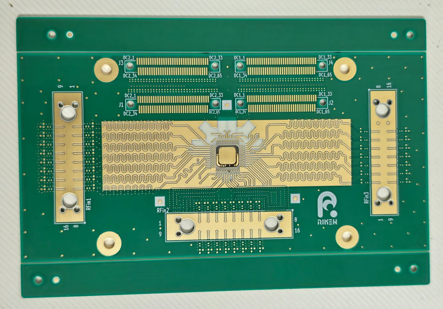
 PRODUCT & PROCESS DETAIL
Board parameters
- Product Model
- 10H79505B0
- PCB Type
- High-Frequency Microwave Multilayer PCB
- Layer Count
- 10 Layers
- Base Material
- Rogers 4350B
- Finished Board Thickness
- 1.60 mm
- Inner Layer Copper Weight
- 0.5 oz
- Outer Layer Copper Weight
- 1 oz
- Minimum Trace Width
- 5.5 mil
- Minimum Trace Spacing
- 3.5 mil
- Minimum Hole Diameter
- 0.20 mm
- Hole Aspect Ratio
- 8:1
- Surface Finish
- NiPdAu (Nickel-Palladium-Gold)
- Application Area
- 5G Communication
- Special Structural Process
- Two-Level Stepped Structure
- Via Filling Process
- Resin Plugging
- Special Via Structure
- Crossed Blind Vias
- High-Frequency Circuit Process
- Microwave Signal Lines
- Visible Circuit Layout
- Symmetrical Serpentine Microwave Traces
- Solder Mask Color
- Green
- Key Manufacturing Processes
- High-Frequency Laminate Processing, Stepped Structure Fabrication, Blind Via Processing, Resin Plugging and Precision Microwave Trace Fabrication
- Primary Manufacturing Challenges
- Multilayer Alignment, Complex Via Interconnections, Stepped Structure Processing, Fine-Line Dimensional Control and High-Frequency Material Fabrication
About this board
Potential Applications and Industry Solutions
This type of high-frequency multilayer PCB is suitable for 5G communication infrastructure, RF transceiver modules, microwave signal-processing equipment, wireless communication systems and specialized RF testing platforms.
It is particularly relevant to telecommunications equipment manufacturers, RF and microwave engineering companies, wireless module developers and communication hardware OEMs requiring complex multilayer interconnections and reliable high-frequency circuit fabrication.
JETFGO supports customized microwave PCB manufacturing, including high-frequency laminate processing, stepped structures, resin-plugged vias and precision signal routing, helping customers move from engineering validation and NPI to volume production.