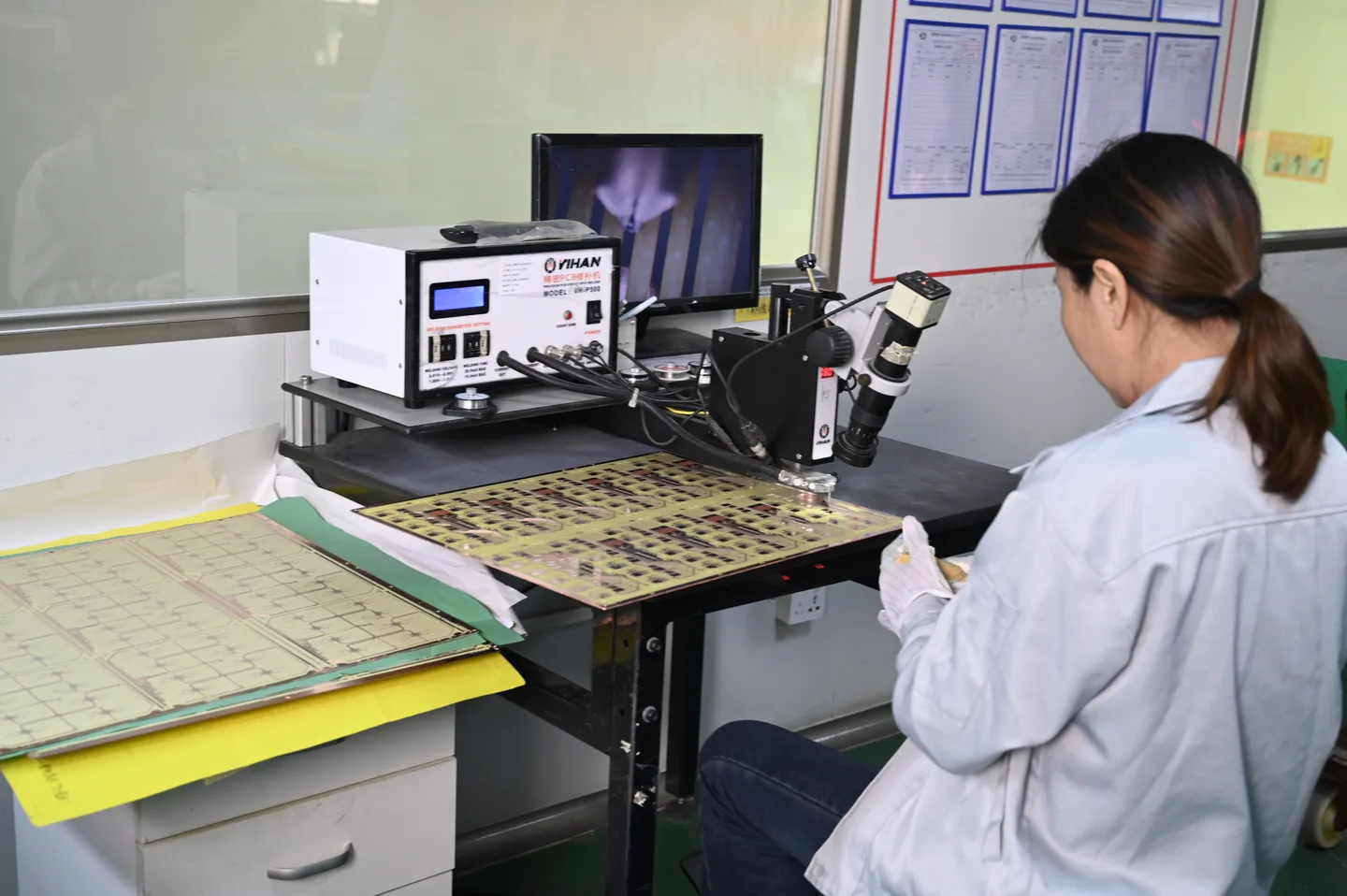
 PRODUCT & PROCESS DETAIL
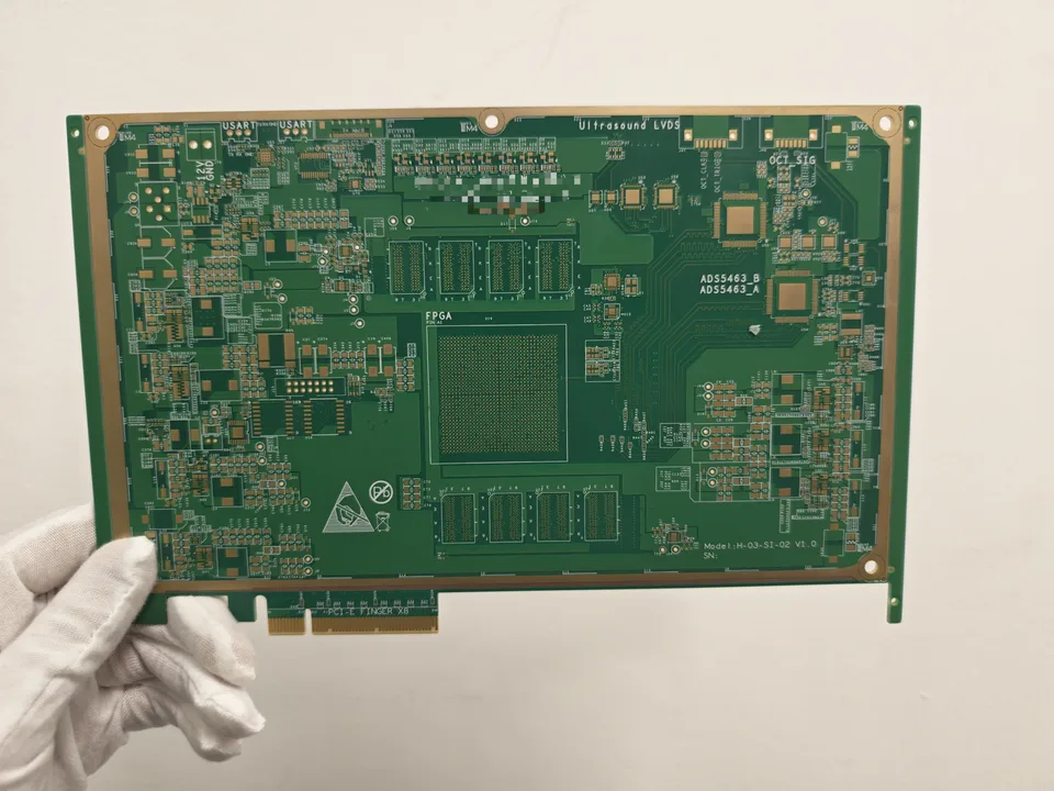
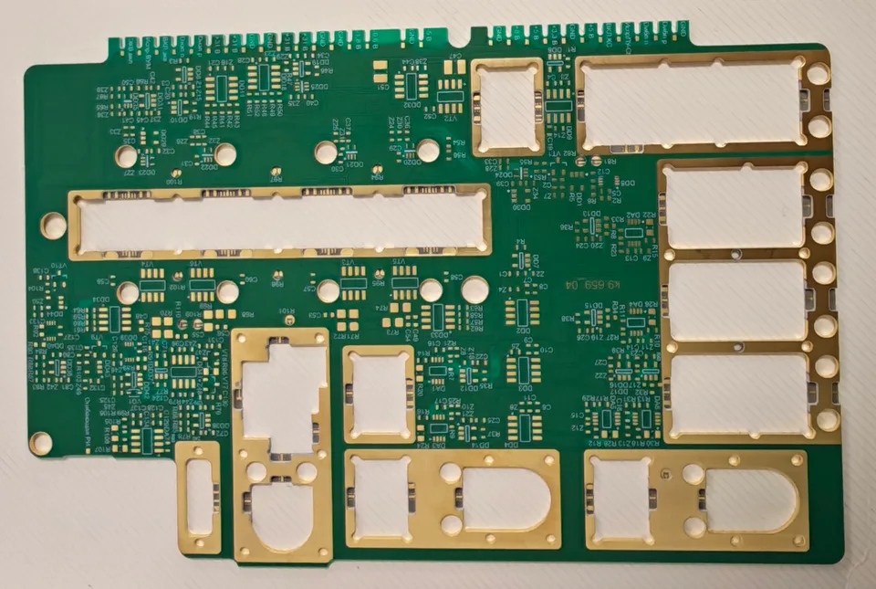
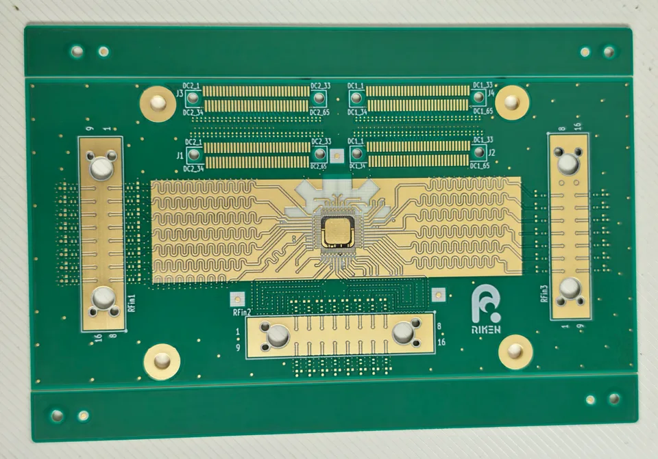
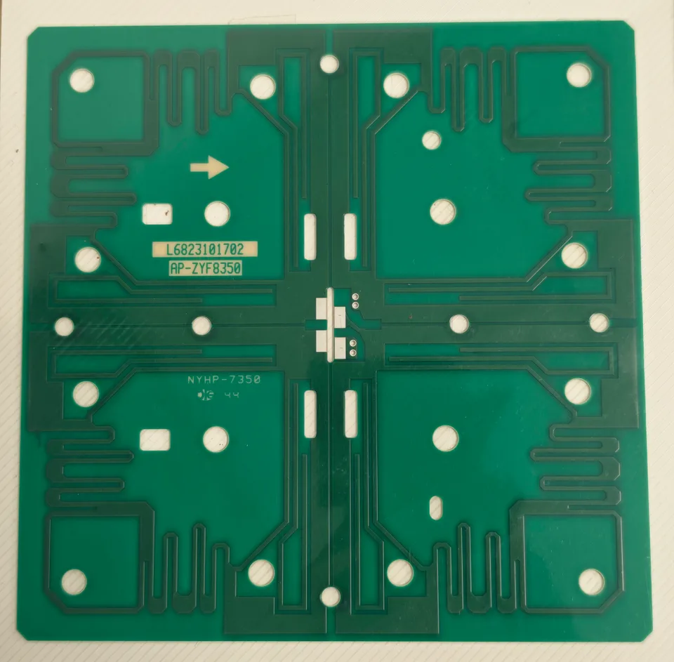
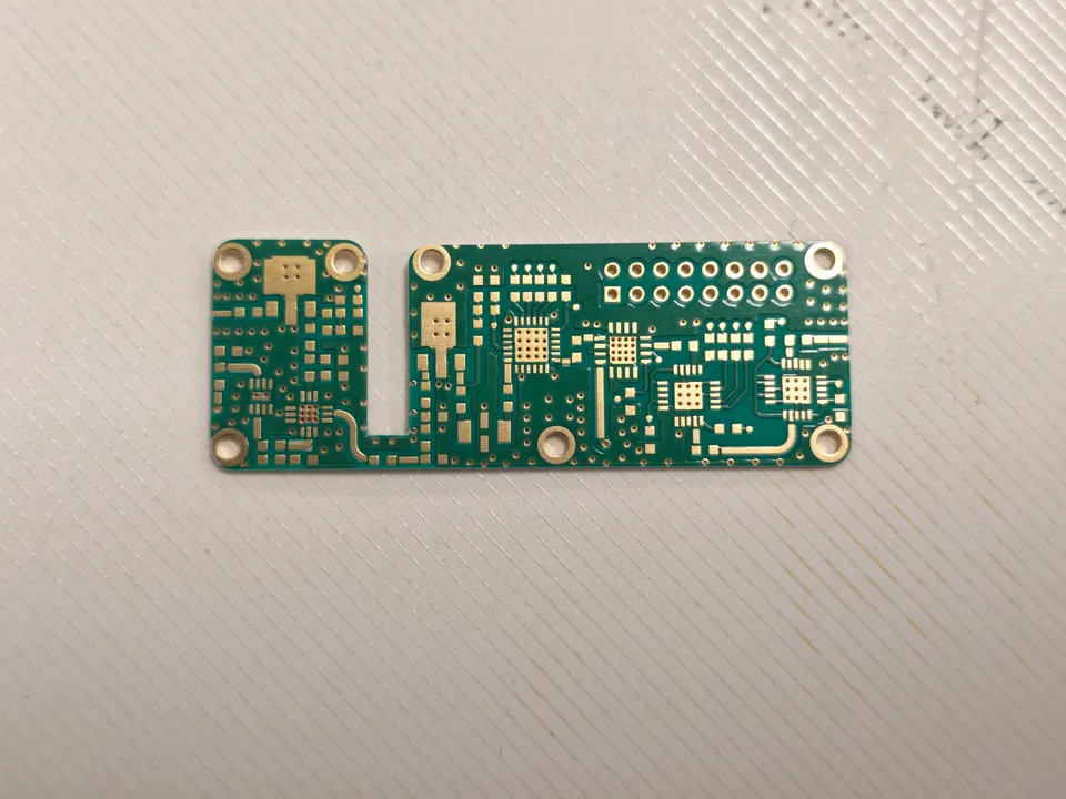
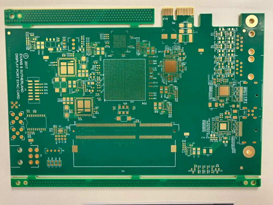
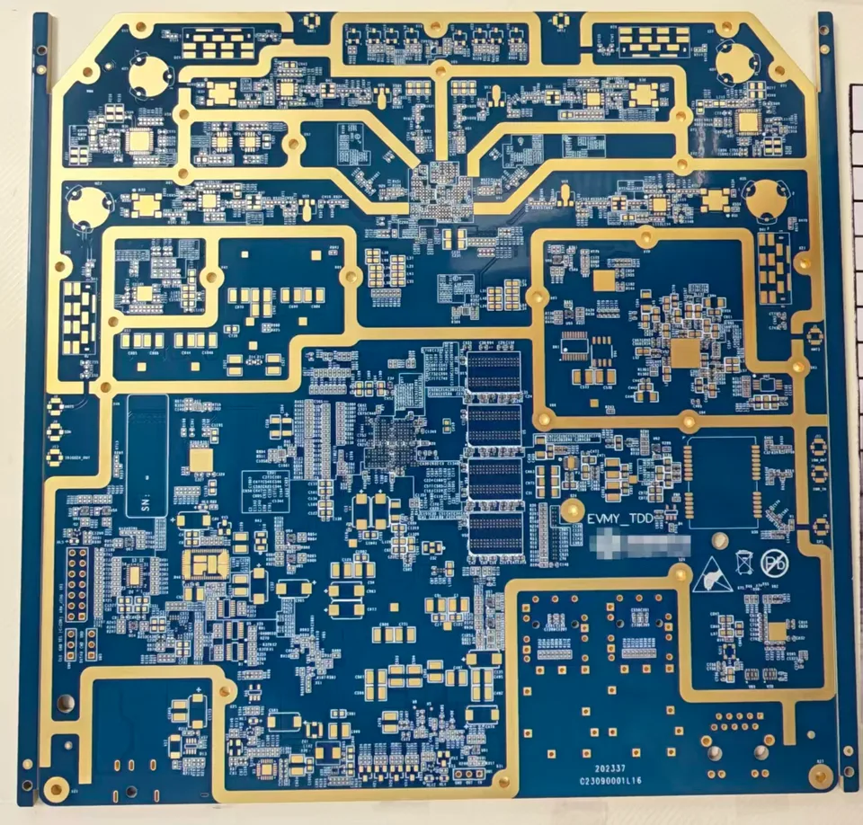
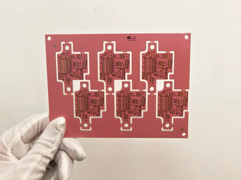
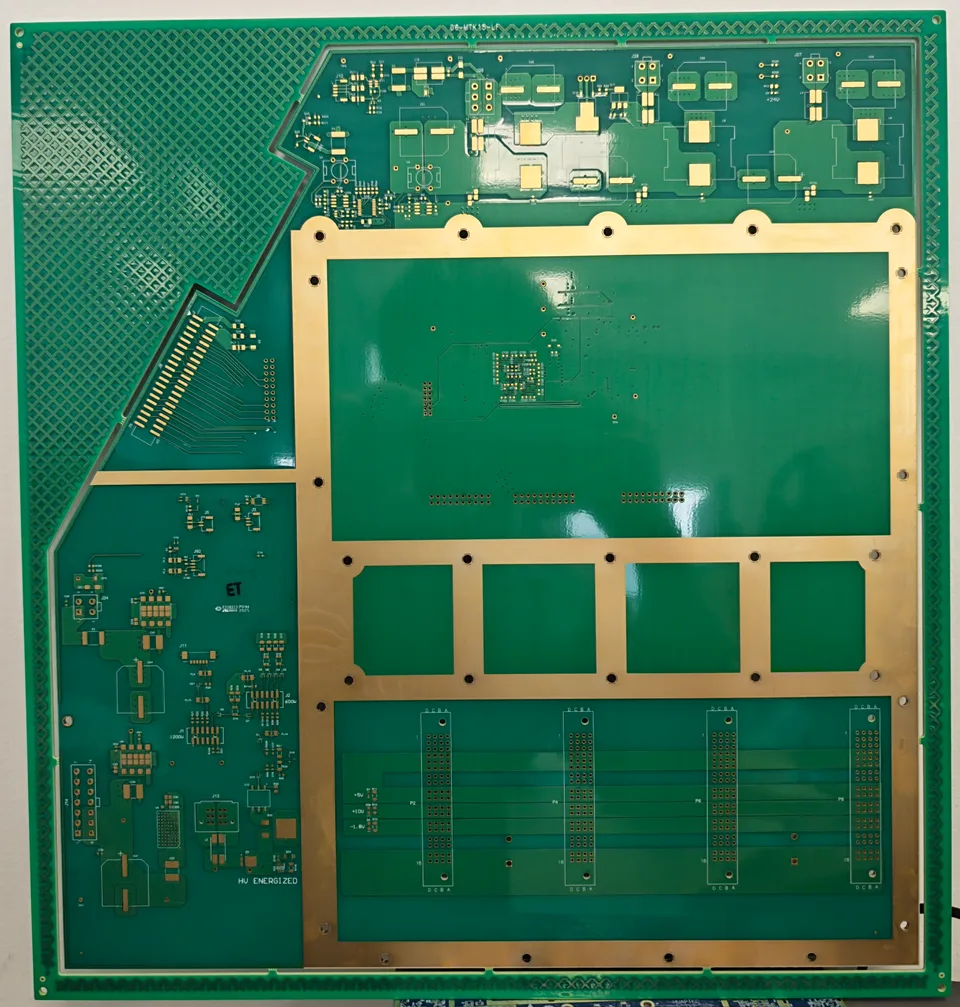
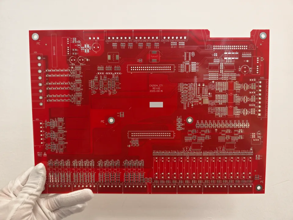
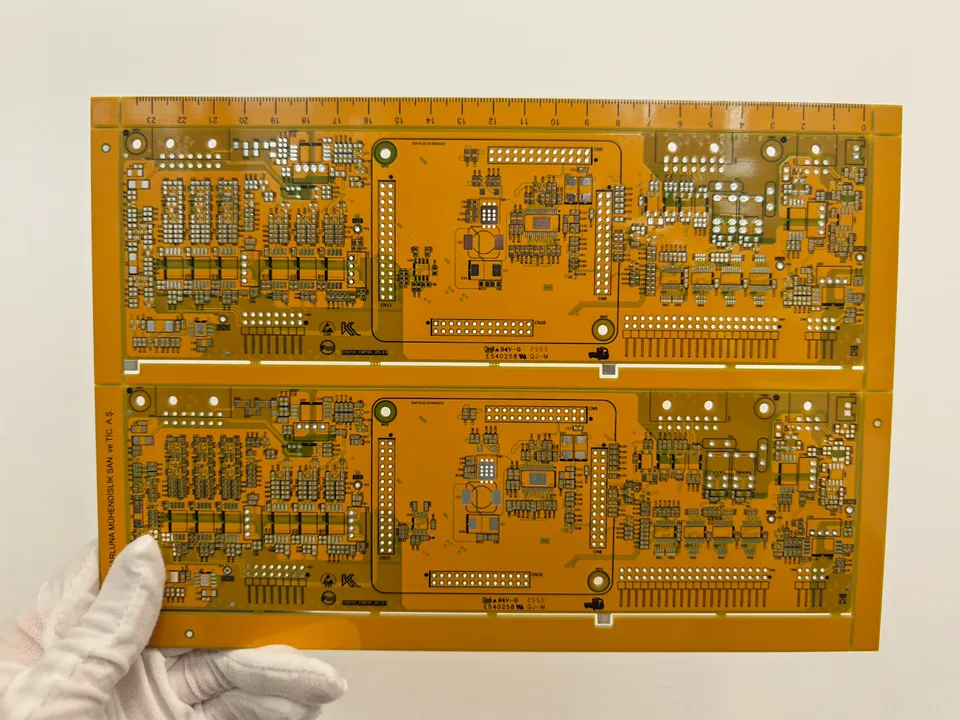
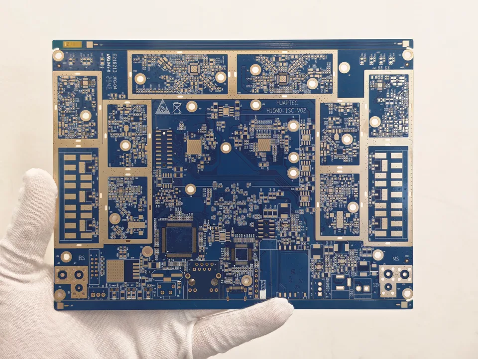
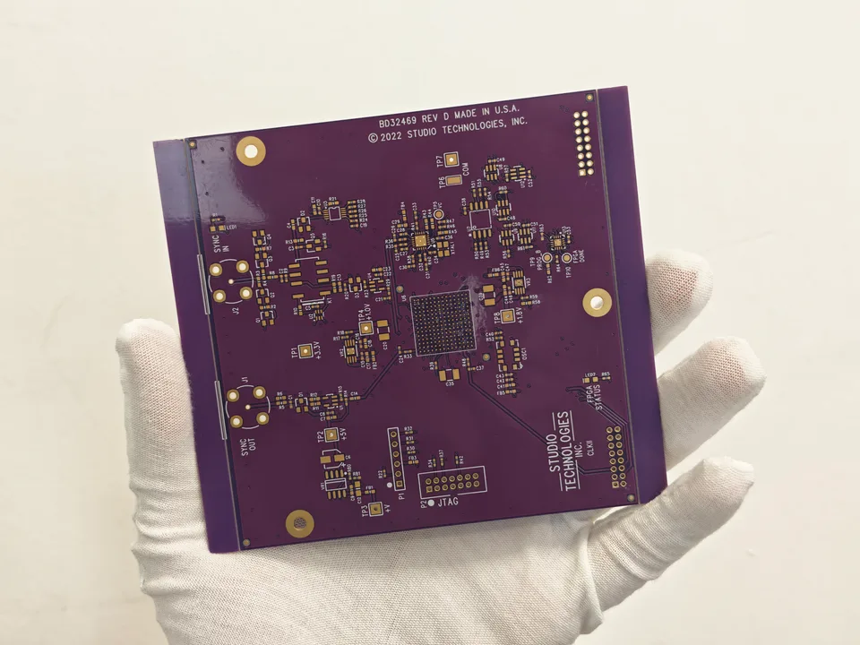
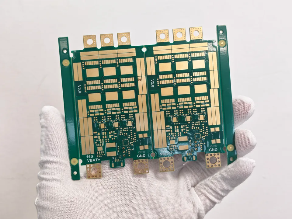
16-Layer High-Density FPGA PCB with Fine-Line Routing and Gold Fingers (119100)
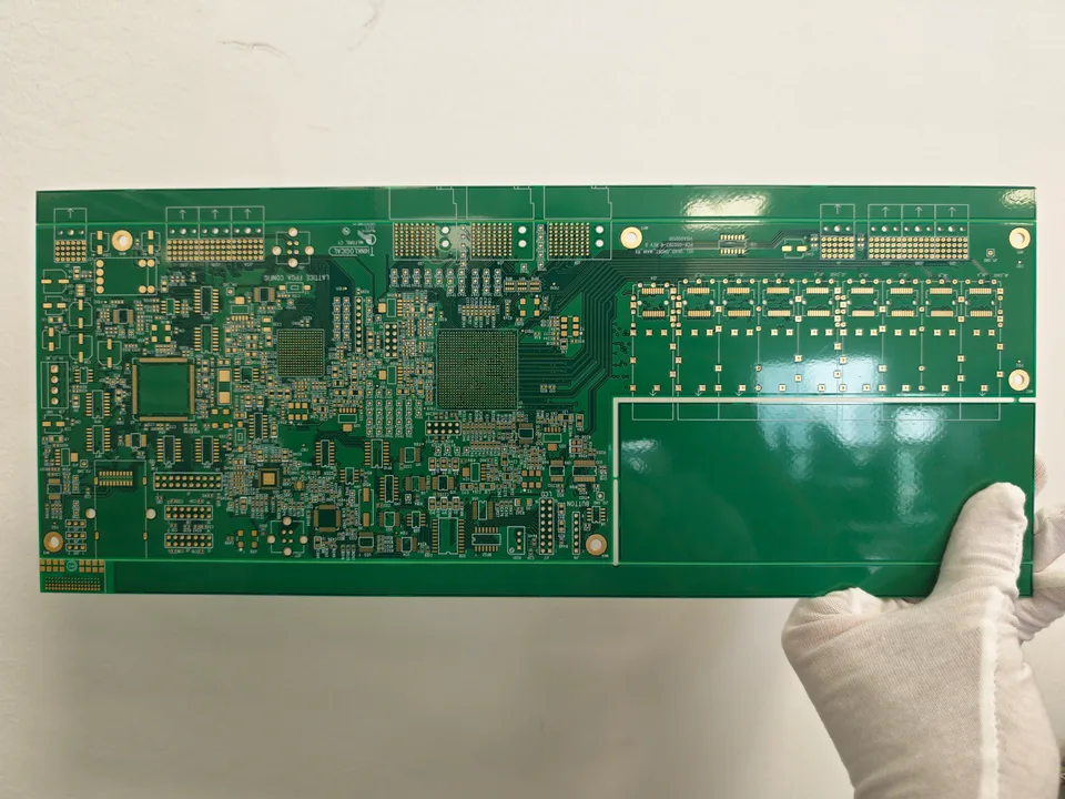
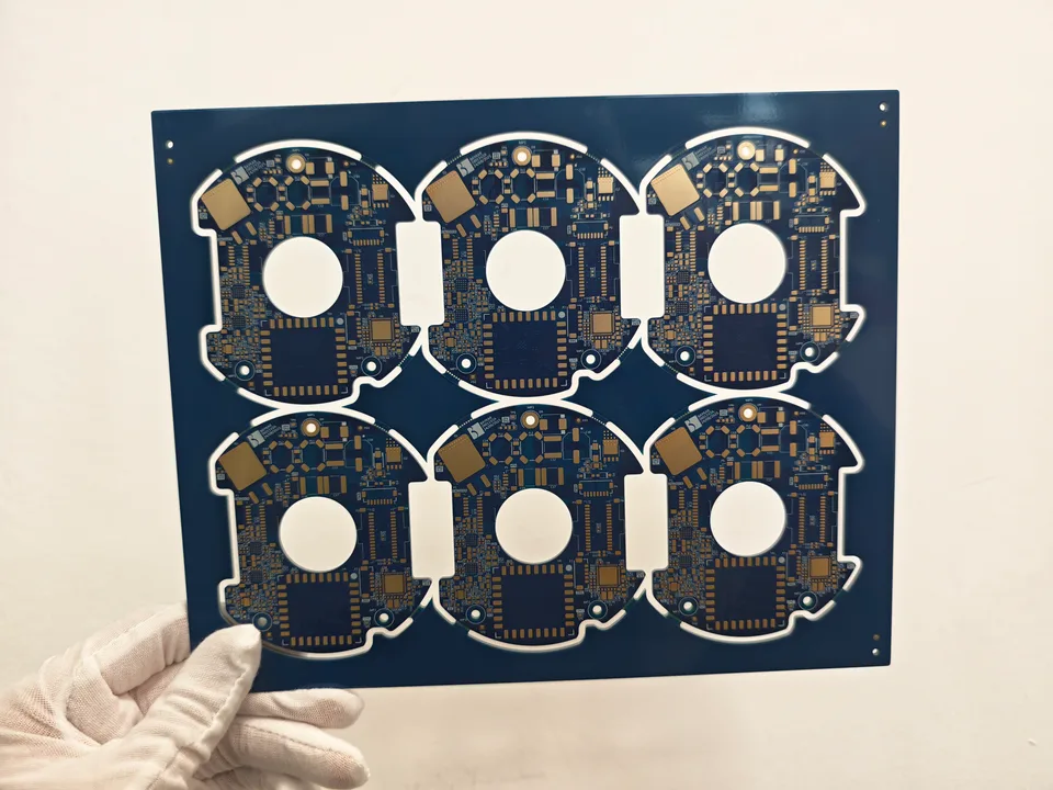
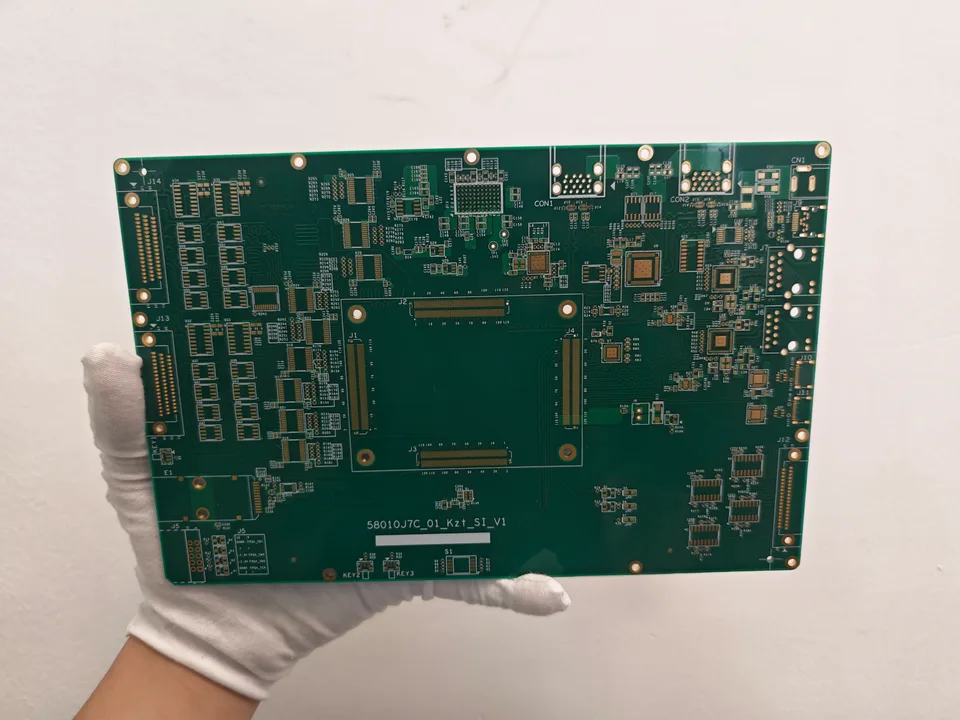
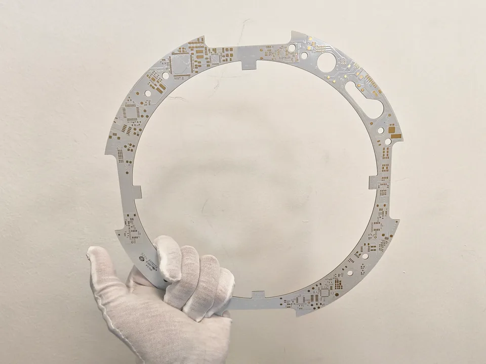
A complex multilayer circuit board featuring dense FPGA interconnections, precision component footprints and high-speed interface routing. Its manufacturing process combines fine-line circuitry, controlled-impedance requirements and specialized connector finishing, demonstrating JETFGO's experience in high-density electronic hardware fabrication.
Collapse
- Product Reference
- 119100
- PCB Type
- High-Density FPGA Multilayer PCB
- Layer Count
- 16 Layers
Less specifications
- Base Material
- FR-4 (Shengyi S1000-2M)
- Glass Transition Temperature (Tg)
- 180°C
- Finished Board Thickness
- 1.70 mm
- Inner Layer Copper Weight
- 0.5 oz
- Outer Layer Copper Weight
- 1 oz
- Inner Layer Trace Width / Spacing
- 3 / 3.98 mil
- Outer Layer Trace Width / Spacing
- 3 / 3.98 mil
- Hole-to-Trace Clearance
- 7.5 mil
- Minimum Hole Diameter
- 0.20 mm
- Plated Hole Copper Thickness
- 20 μm
- Surface Finish
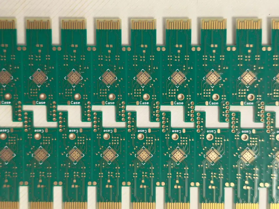
- ENIG + Gold-Plated Edge Fingers
- Gold Finger Plating Thickness
- 15 μin (As Specified)
- Solder Mask Color
- Green
- Solder Mask Material
- PSR-4000 G23K
- Silkscreen Color
- White
- Impedance Control
- Required
- PCB Connection Interface
- PCIe x8 Edge Connector
- Visible Circuit Features
- High-Density FPGA BGA Pads, Fine-Line Routing and Dense Component Footprints
- Visible Signal Interfaces
- Ultrasound LVDS, USART and ADS5463_A/B
- SET Dimensions
- 241.14 × 152.41 mm
- Drilled Hole Count
- 5,243
- Electrical Test Points
- 5,797
- Hole Density
- 142,659 Holes/m²
- Electrical Testing
- Dedicated Test Fixture
- PCB Profiling
- CNC Routing
- Via Processing
- Aluminum-Sheet Via Plugging Process (Per Engineering Record)
- Key Manufacturing Processes
- Multilayer Lamination, Fine-Line Etching, Impedance Control, Precision Drilling, ENIG Finishing and Gold-Finger Plating
- Primary Manufacturing Challenges
- 16-Layer Registration, Fine-Line Dimensional Control, Dense Interconnections, Via Metallization and Connector Plating Consistency