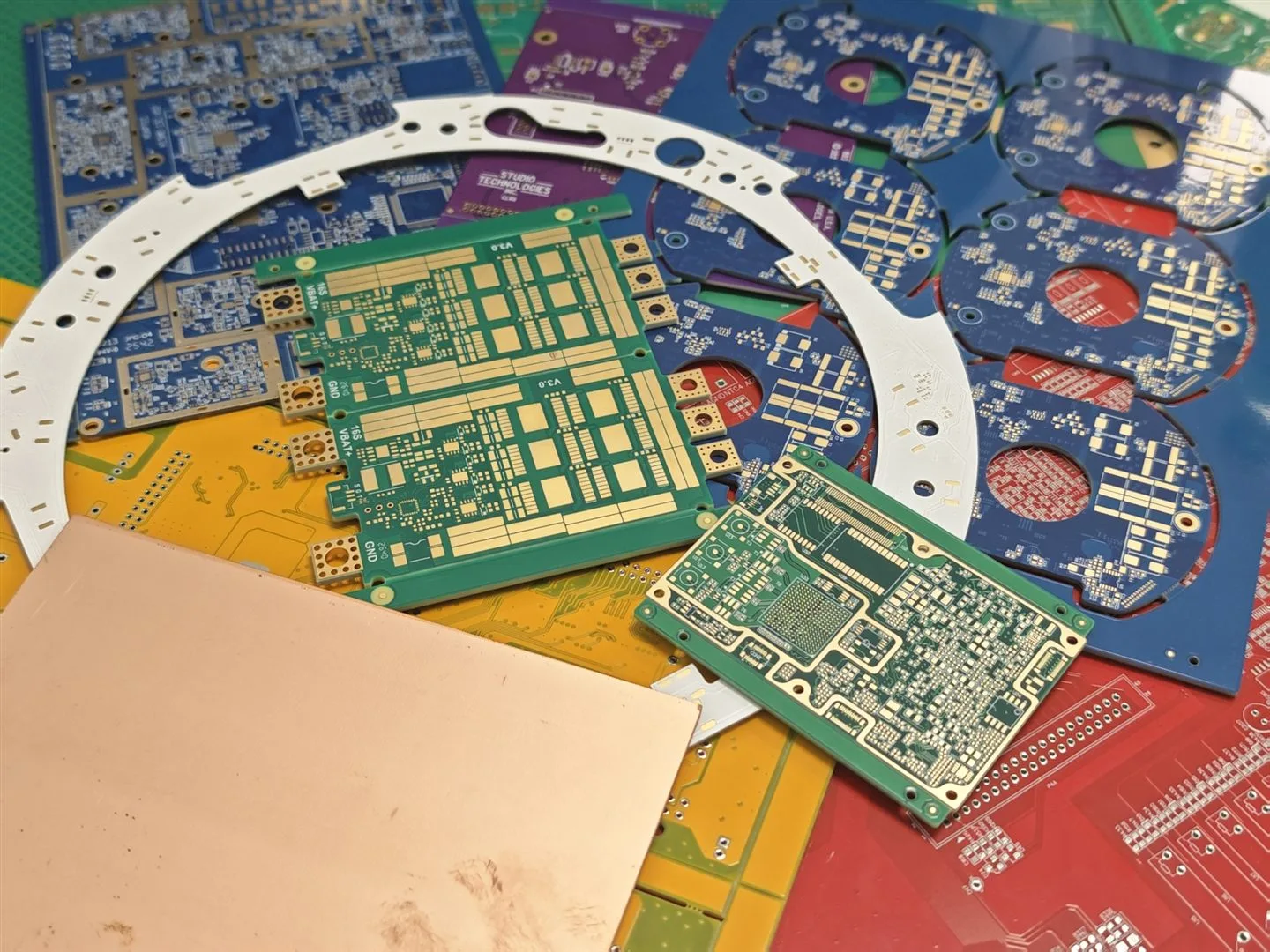
PCB ENGINEERING LIBRARY / Real PCB Samples & Customer Cases

Real PCB Samples & Customer Cases

Explore real PCB board photos, project examples and available manufacturing specifications.

33
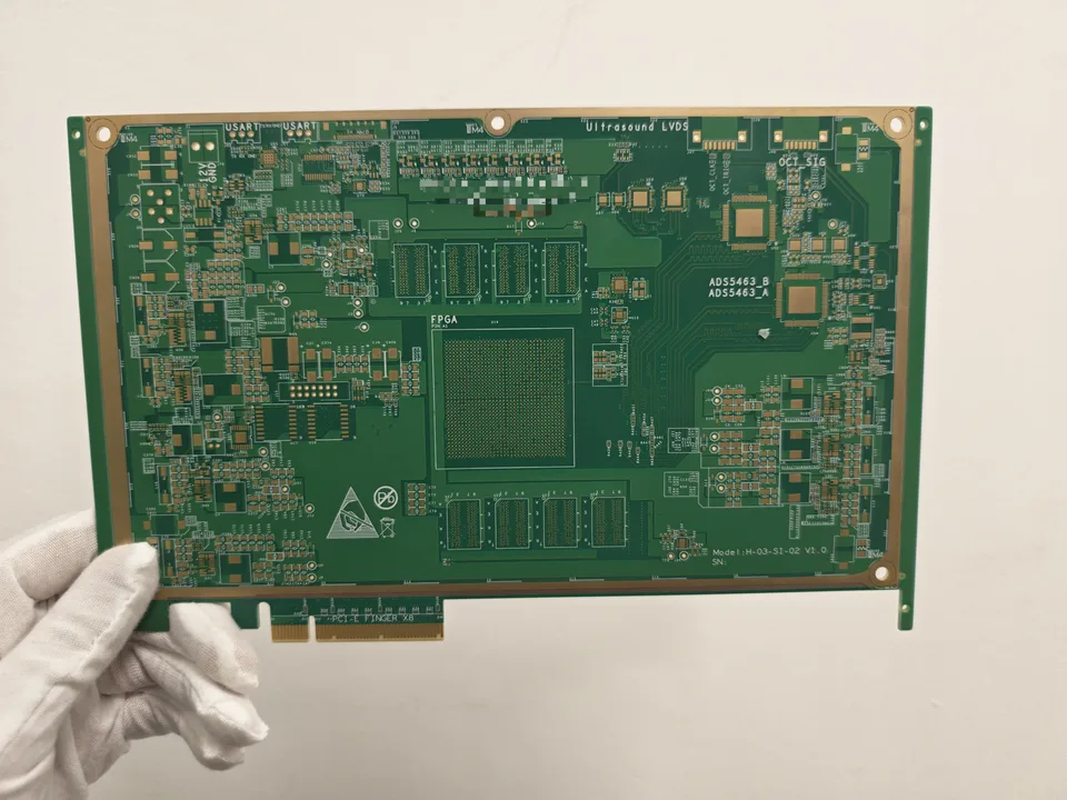
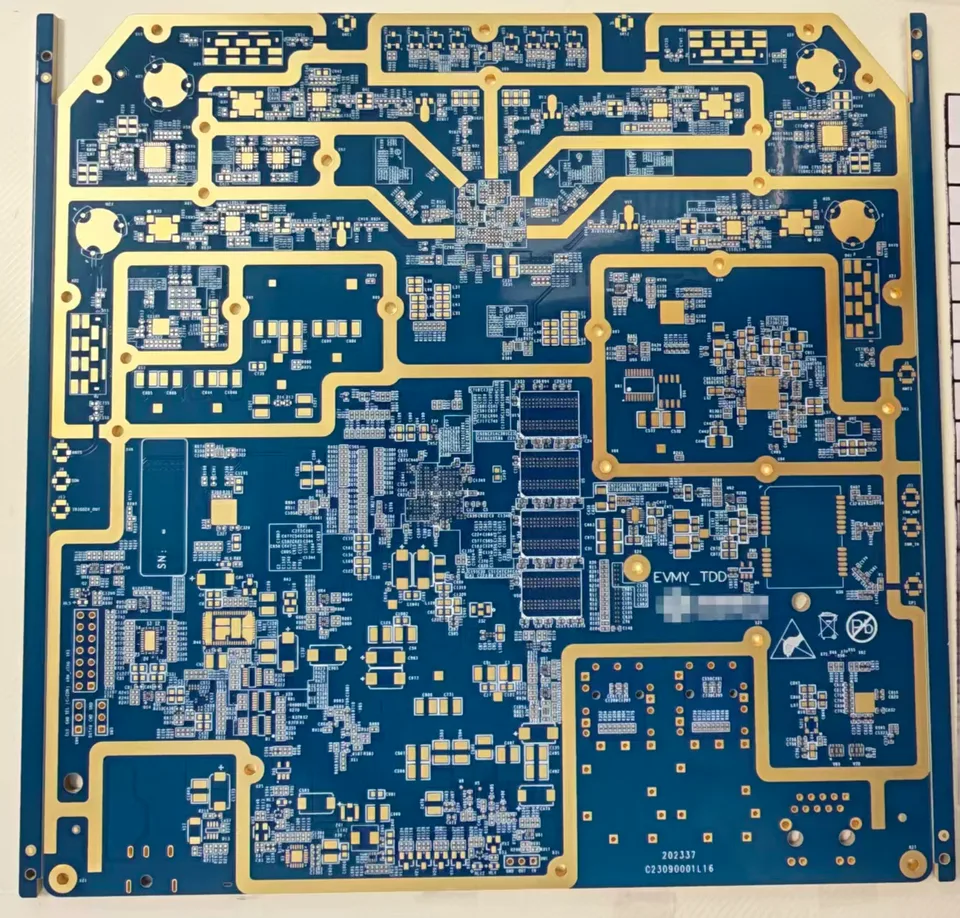
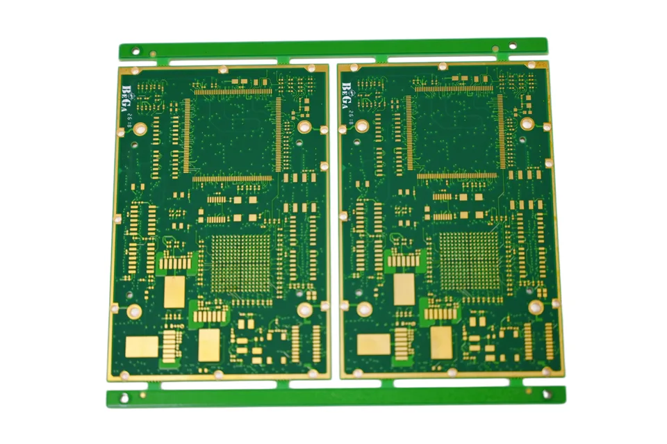
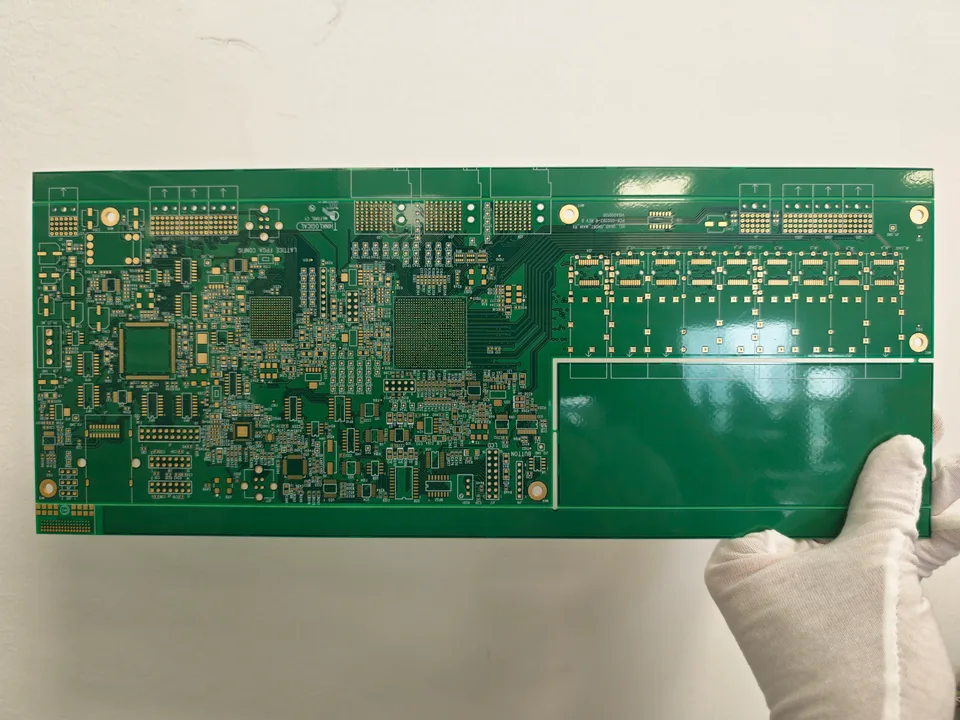
16-Layer High-Density FPGA PCB with Fine-Line Routing and Gold Fingers (119100)
JETFGO / 01

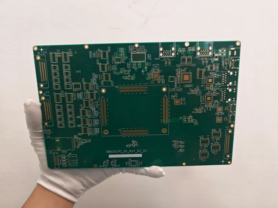
16-Layer High-Density FPGA PCB with Fine-Line Routing and Gold Fingers (119100)

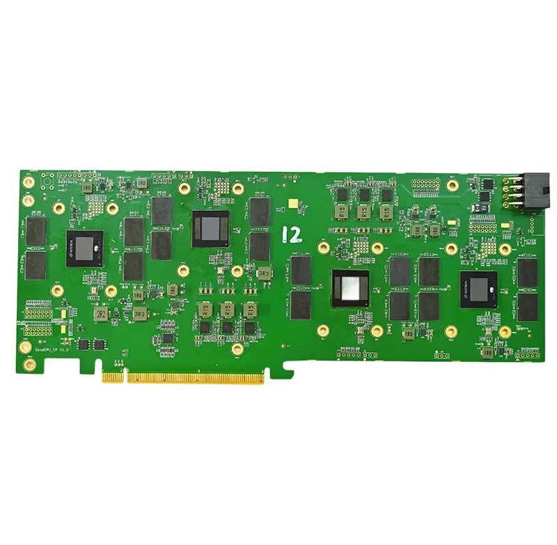
A complex multilayer circuit board featuring dense FPGA interconnections, precision component footprints and high-speed interface routing. Its manufacturing process combines fine-line circuitry, controlled-impedance requirements and specialized connector finishing, demonstrating JETFGO's experience in high-density electronic hardware fabrication.

ExpandCollapse
Product Reference
119100
PCB Type
High-Density FPGA Multilayer PCB
Layer Count
16 Layers
More specificationsLess specifications
Base Material
FR-4 (Shengyi S1000-2M)
Glass Transition Temperature (Tg)
180°C
Finished Board Thickness
1.70 mm
Inner Layer Copper Weight
0.5 oz
Outer Layer Copper Weight
1 oz
Inner Layer Trace Width / Spacing
3 / 3.98 mil
Outer Layer Trace Width / Spacing
3 / 3.98 mil
Hole-to-Trace Clearance
7.5 mil
Minimum Hole Diameter
0.20 mm
Plated Hole Copper Thickness
20 μm
Surface Finish
ENIG + Gold-Plated Edge Fingers
Gold Finger Plating Thickness
15 μin (As Specified)
Solder Mask Color
Green
Solder Mask Material
PSR-4000 G23K
Silkscreen Color
White
Impedance Control
Required
PCB Connection Interface
PCIe x8 Edge Connector
Visible Circuit Features
High-Density FPGA BGA Pads, Fine-Line Routing and Dense Component Footprints
Visible Signal Interfaces
Ultrasound LVDS, USART and ADS5463_A/B
SET Dimensions
241.14 × 152.41 mm
Drilled Hole Count
5,243
Electrical Test Points
5,797
Hole Density
142,659 Holes/m²
Electrical Testing
Dedicated Test Fixture
PCB Profiling
CNC Routing
Via Processing
Aluminum-Sheet Via Plugging Process (Per Engineering Record)
Key Manufacturing Processes
Multilayer Lamination, Fine-Line Etching, Impedance Control, Precision Drilling, ENIG Finishing and Gold-Finger Plating
Primary Manufacturing Challenges
16-Layer Registration, Fine-Line Dimensional Control, Dense Interconnections, Via Metallization and Connector Plating Consistency
View details
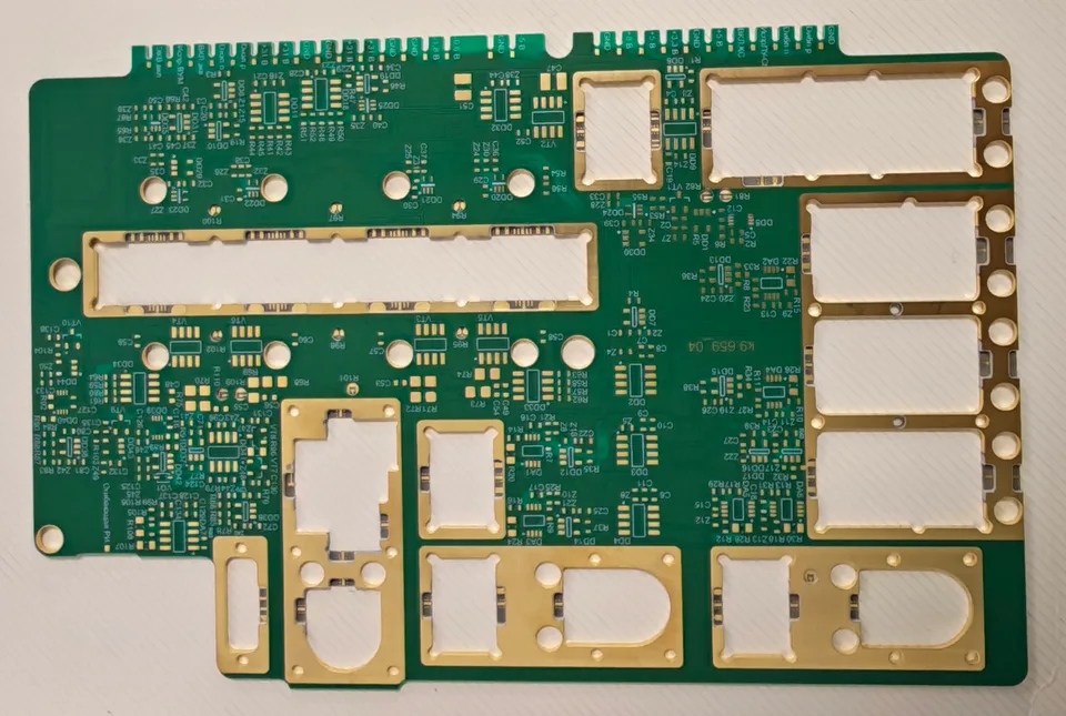
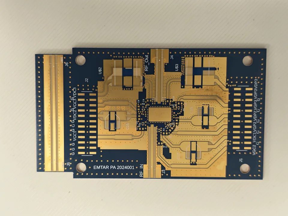
4-Layer Panasonic M6 RF PCB with Copper Inlay and Reinforcement (04H84792A0)
JETFGO / 02

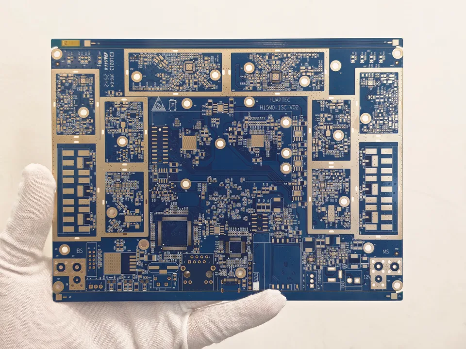
4-Layer Panasonic M6 RF PCB with Copper Inlay and Reinforcement (04H84792A0)

A specialized multilayer circuit board combining precision RF signal routing with embedded copper features and reinforced mechanical structures. Its manufacturing process demonstrates JETFGO's capabilities in advanced laminate processing, localized copper integration and complex PCB fabrication for demanding electronic applications.

ExpandCollapse
Product Model
04H84792A0
PCB Type
RF PCB with Copper Inlay and Reinforcement
Layer Count
4 Layers
More specificationsLess specifications
Base Material
Panasonic M6
Finished Board Thickness
1.90 mm
Inner Layer Finished Copper Weight
0.5 oz
Outer Layer Finished Copper Weight
1 oz
Copper Configuration
0.5 oz Inner / 1 oz Outer
Trace Width
19 mil
Trace Spacing
5.5 mil
Minimum Hole Diameter
0.25 mm
Hole Aspect Ratio
2.8:1 (Process Card Value; Verification Required)
Surface Finish
NiPdAu (Nickel-Palladium-Gold)
Special Manufacturing Process
Copper Inlay
Mechanical Reinforcement
Copper Plate Reinforcement
Visible RF Connections
RF_IN and RF_OUT
Visible Board Marking
EMTAR PA 2024001
Visible Circuit Features
RF Signal Routing, Wide Copper Areas, Multiple Connection Pads and Mounting Holes
Solder Mask Color
Dark Blue
Silkscreen Color
White
Key Manufacturing Processes
Panasonic M6 Laminate Processing, Copper Inlay Integration, Copper Reinforcement, Precision Circuit Etching and NiPdAu Finishing
Primary Manufacturing Challenges
Embedded Copper Integration, Lamination Compatibility, Reinforcement Alignment, Circuit Dimensional Control and Surface Finish Consistency
View details
10-Layer Heavy Copper HDI Power Control PCB (10C85585A0)
JETFGO / 03

10-Layer Heavy Copper HDI Power Control PCB (10C85585A0)

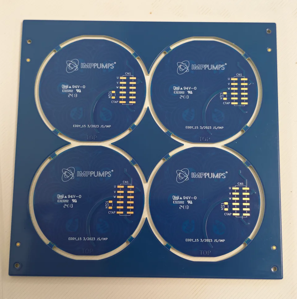
A specialized multilayer circuit board combining substantial copper thickness with high-density interconnections and buried via technology. Its manufacturing process demonstrates JETFGO's ability to integrate heavy copper fabrication, complex multilayer structures and precision interconnection processing for demanding power electronics applications.

ExpandCollapse
Product Model
10C85585A0
PCB Type
Heavy Copper HDI Power Control PCB
Layer Count
10 Layers
More specificationsLess specifications
Base Material
Shengyi S1000-2M
Finished Board Thickness
2.60 mm
Inner Layer Finished Copper Weight
3 oz
Outer Layer Finished Copper Weight
2 oz
Copper Configuration
3 oz Inner Layers / 2 oz Outer Layers
Minimum Trace Width
12.8 mil
Minimum Trace Spacing
7.4 mil
Minimum Hole Diameter
0.35 mm
Hole Aspect Ratio
7.43:1
Surface Finish
ENIG (Electroless Nickel Immersion Gold)
Application Area
Power Control
HDI Technology
First-Order HDI
Special Via Technology
Buried Vias
Special Manufacturing Process
Heavy Copper Fabrication
Solder Mask Color
Blue
Silkscreen Color
White
Visible Board Structure
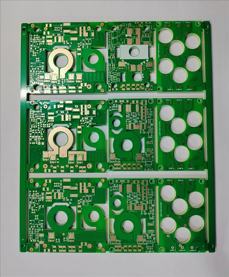
Four Circular PCB Units in a Panel
Visible Electrical Markings
U, V, W, NTC1 and CTAP
Key Manufacturing Processes
Heavy Copper Etching, First-Order HDI Fabrication, Buried Via Processing, Multilayer Lamination and Precision Drilling
Primary Manufacturing Challenges
Heavy Copper Etching Control, Multilayer Registration, Buried Via Interconnections, Lamination Reliability and Hole Metallization
View details
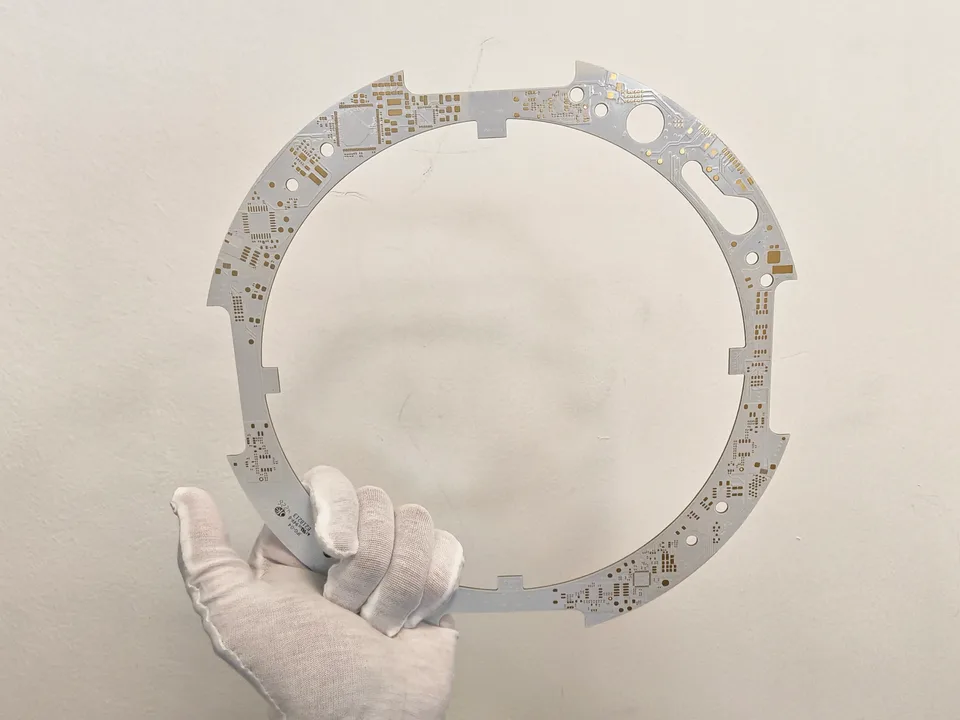
6-Layer HDI Rigid-Flex PCB with Fine-Line Routing and Blind Vias (06M50112A0)
JETFGO / 04

6-Layer HDI Rigid-Flex PCB with Fine-Line Routing and Blind Vias (06M50112A0)

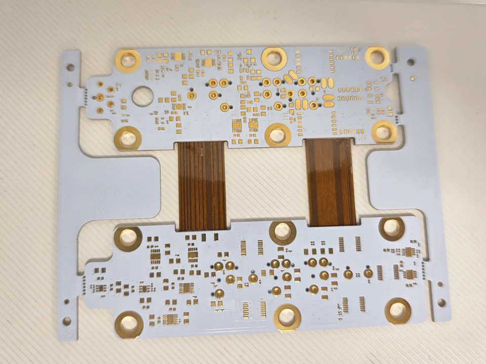
A compact, precision-engineered circuit board combining rigid sections with flexible interconnections. Its complex construction integrates fine-pitch circuitry, advanced via structures and specialized depth-controlled processing, demonstrating JETFGO's manufacturing capabilities in high-density rigid-flex electronics.

ExpandCollapse
Product Model
06M50112A0
PCB Type
HDI Rigid-Flex PCB
Total Layer Count
6 Layers
More specificationsLess specifications
Rigid Section Structure
Layers 1–4
Flexible Section Structure
Layers 5–6
Base Materials
SF202 + High-Tg FR-4
Finished Board Thickness
0.80 mm (As Specified)
Minimum Trace Width
2.9 mil
Minimum Trace Spacing
2.9 mil
Minimum Hole Diameter
0.15 mm
Hole Aspect Ratio
5.33:1
Surface Finishes
ENIG + Immersion Silver
Special PCB Technology
Rigid-Flex Integration + HDI
Via Technology
Blind and Buried Vias
Specified Via Layer Connections
L1–L2 / L2–L6 / L5–L6
Special Hole Process
Stepped Hole Processing
Special Edge Process
Controlled-Depth Beveling
Impedance Control
Required
Visible Rigid Board Appearance
White
Visible Flexible Interconnections
Two Brown Flexible Sections
Visible PCB Features
Fine-Pitch Pads, Plated Mounting Holes and Custom-Shaped Openings
Key Manufacturing Processes
Rigid-Flex Lamination, HDI Fabrication, Fine-Line Etching, Precision Drilling, Stepped Hole Processing and Controlled-Depth Beveling
Primary Manufacturing Challenges
Rigid-to-Flex Transition Control, Multilayer Registration, Fine-Line Dimensional Accuracy, Complex Via Interconnections and Controlled-Depth Processing
View details
24-Layer Panasonic M6 High-Speed PCB with Precision Backdrilling (AA4456)
JETFGO / 05

24-Layer Panasonic M6 High-Speed PCB with Precision Backdrilling (AA4456)

A complex high-layer-count circuit board featuring dense electronic interconnections, precision via structures and demanding signal-routing requirements. Its manufacturing process combines advanced multilayer lamination, high-aspect-ratio drilling, controlled-impedance fabrication and specialized via processing, demonstrating JETFGO's experience in manufacturing sophisticated high-speed electronic hardware.

ExpandCollapse
Product Model
AA4456
PCB Type
High-Speed High-Layer-Count PCB
Layer Count
24 Layers
More specificationsLess specifications
Base Material
Panasonic M6 High-Speed Laminate
Finished Board Thickness
3.00 mm
Minimum Trace Width
3.5 mil
Minimum Trace Spacing
4 mil
Minimum Hole Diameter
0.25 mm
Hole Aspect Ratio
12:1
BGA Feature Size
0.30 mm
Surface Finish
ENIG (Electroless Nickel Immersion Gold)
Solder Mask Color
Green
Special PCB Structure
High-Layer-Count Multilayer Construction
Impedance Control
Differential and Single-Ended Impedance Requirements
Differential Impedance Groups
32 Groups
Backdrilling Requirements
12 Backdrilling Groups
Special Drilling Process
Controlled-Depth Backdrilling
Inner-Layer Hole-to-Trace Clearance
6.7 mil Minimum
Via Filling Process
Resin Plugging
Special Material Requirement
Panasonic M6 Laminate with Inner-Layer Construction Requirements
Key Manufacturing Processes
Multilayer Lamination, High-Aspect-Ratio Drilling, Precision Backdrilling, Impedance Control and Resin Via Plugging
Primary Manufacturing Challenges
24-Layer Registration, High-Aspect-Ratio Hole Metallization, Backdrilling Depth Control, Fine-Line Fabrication and Impedance Consistency
View details
6-Layer Rogers 4350B High-Frequency PCB with Stepped Structure (06H76466C0)
JETFGO / 06

6-Layer Rogers 4350B High-Frequency PCB with Stepped Structure (06H76466C0)

A specialized multilayer circuit board featuring complex mechanical openings, precision connection areas and customized structural processing. Its combination of high-frequency laminate fabrication, intricate PCB profiling and selective surface finishing demonstrates JETFGO's ability to manufacture demanding RF circuit designs.

ExpandCollapse
Product Model
06H76466C0
PCB Type
High-Frequency Stepped Multilayer PCB
Layer Count
6 Layers
More specificationsLess specifications
Base Material
Rogers 4350B
Finished Board Thickness
1.18 mm
Inner Layer Copper Weight
0.5 oz
Outer Layer Copper Weight
1 oz
Minimum Trace Width
11.3 mil
Minimum Trace Spacing
3.2 mil
Minimum Hole Diameter
0.25 mm
Hole Aspect Ratio
4.32:1 (Process Card Specification)
Surface Finish
NiPdAu (Nickel-Palladium-Gold)
Application Area
5G Communication
Special Manufacturing Process
Two-Level Stepped Structure
Visible Board Features
Large Custom Cutouts, Non-Standard Board Profile and Multiple Connection Pads
Solder Mask Color
Green
Key Manufacturing Processes
Rogers High-Frequency Laminate Processing, Stepped Structure Fabrication, Precision Drilling and Custom PCB Profiling
Primary Manufacturing Challenges
Stepped Structure Dimensional Control, High-Frequency Material Processing, Narrow Trace Spacing and Complex Cutout Accuracy
View details
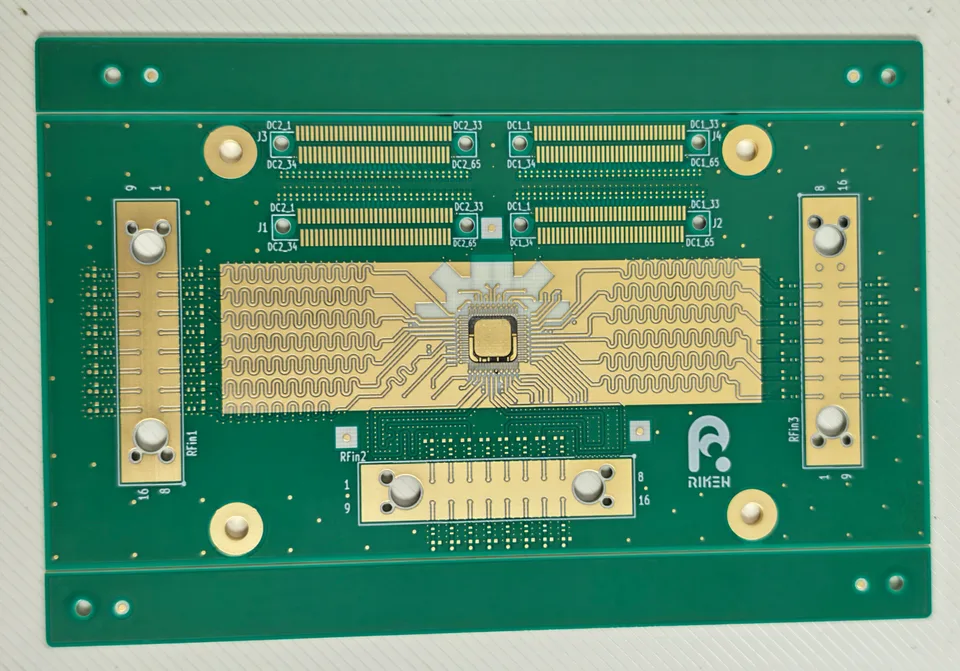
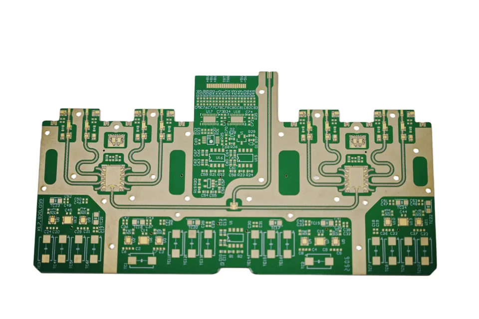
10-Layer Rogers 4350B Microwave PCB with Stepped Structure and Blind Vias (10H79505B0)
JETFGO / 07

10-Layer Rogers 4350B Microwave PCB with Stepped Structure and Blind Vias (10H79505B0)

A precision high-frequency multilayer circuit board featuring symmetrical microwave signal routing, dense interconnections and specialized structural processing. The combination of advanced laminate fabrication, complex via structures and controlled conductor geometry demonstrates JETFGO's manufacturing capabilities for demanding RF and communication electronics.

ExpandCollapse
Product Model
10H79505B0
PCB Type
High-Frequency Microwave Multilayer PCB
Layer Count
10 Layers
More specificationsLess specifications
Base Material
Rogers 4350B
Finished Board Thickness
1.60 mm
Inner Layer Copper Weight
0.5 oz
Outer Layer Copper Weight
1 oz
Minimum Trace Width
5.5 mil
Minimum Trace Spacing
3.5 mil
Minimum Hole Diameter
0.20 mm
Hole Aspect Ratio
8:1
Surface Finish
NiPdAu (Nickel-Palladium-Gold)
Application Area
5G Communication
Special Structural Process
Two-Level Stepped Structure
Via Filling Process
Resin Plugging
Special Via Structure
Crossed Blind Vias
High-Frequency Circuit Process
Microwave Signal Lines
Visible Circuit Layout
Symmetrical Serpentine Microwave Traces
Solder Mask Color
Green
Key Manufacturing Processes
High-Frequency Laminate Processing, Stepped Structure Fabrication, Blind Via Processing, Resin Plugging and Precision Microwave Trace Fabrication
Primary Manufacturing Challenges
Multilayer Alignment, Complex Via Interconnections, Stepped Structure Processing, Fine-Line Dimensional Control and High-Frequency Material Fabrication
View details
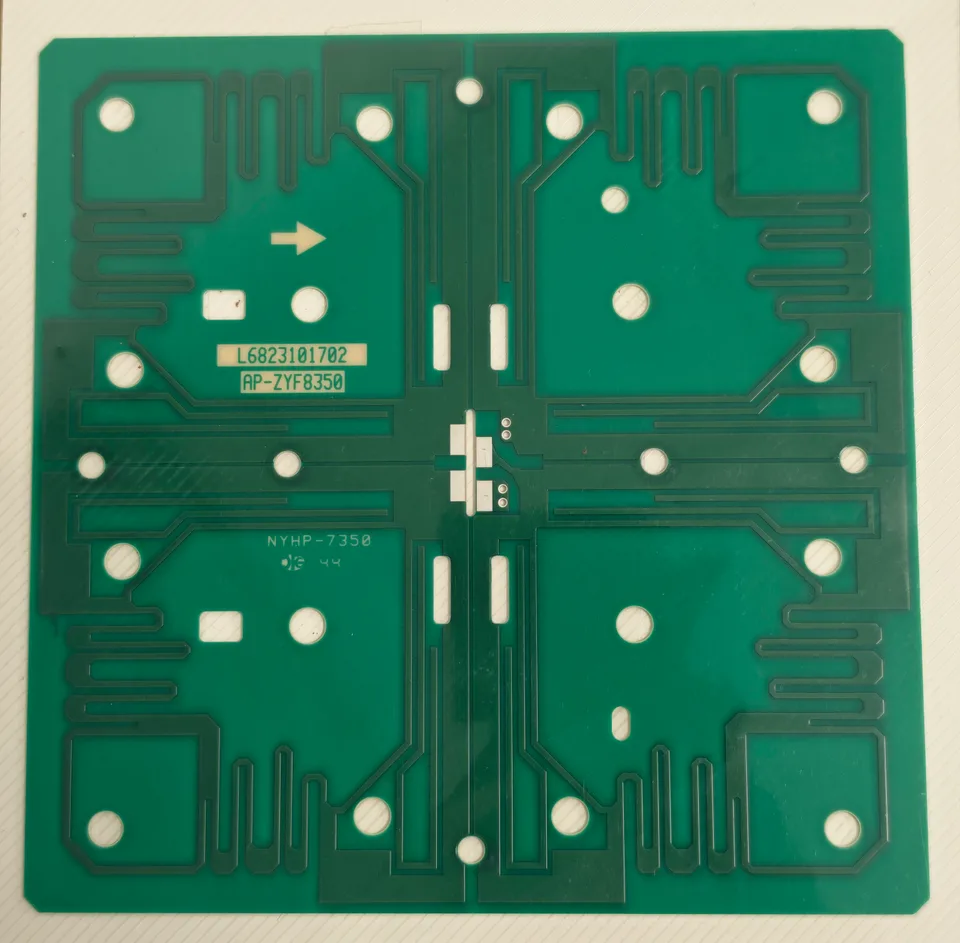
2-Layer 5G Microstrip RF PCB with Precision Trace Width Control (02F79548A0)
JETFGO / 08

2-Layer 5G Microstrip RF PCB with Precision Trace Width Control (02F79548A0)

A specialized RF circuit board featuring symmetrical microstrip transmission lines and carefully controlled conductor geometry. Its manufacturing process emphasizes consistent copper patterning, precise signal-trace dimensions and controlled solder mask application, demonstrating JETFGO's capabilities in high-frequency PCB fabrication.

ExpandCollapse
Product Model
02F79548A0
PCB Type
5G Microstrip RF PCB
Layer Count
2 Layers
More specificationsLess specifications
Base Material
NYHP-7350
Finished Board Thickness
0.63 mm
Finished Copper Weight
1.5 oz
Trace Width
19.7 mil
Trace Spacing
10 mil
Minimum Hole Diameter
0.45 mm
Hole Aspect Ratio
1.29:1 (Process Card Specification)
Surface Finish
Immersion Tin
Application Area
5G Signal Communication
Special Circuit Structure
Microstrip Transmission Lines
Visible Circuit Layout
Symmetrical RF Traces and Serpentine Routing
General Trace Width Tolerance
±8%
High-Frequency Signal Trace Width Tolerance
±6%
Solder Mask Processing
Single-Pass Printing Required
Solder Mask Color
Green
Key Manufacturing Processes
Microstrip Circuit Patterning, Precision Copper Etching, Trace Width Control and Immersion Tin Finishing
Primary Manufacturing Challenges
RF Trace Dimensional Accuracy, Consistent Conductor Geometry and Single-Pass Solder Mask Control
View details
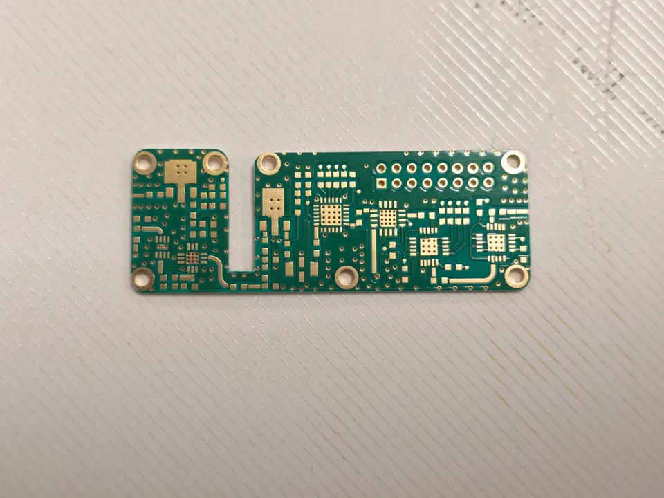
4-Layer Hybrid RF HDI PCB with Precision Interconnects (04C76237)
JETFGO / 09

4-Layer Hybrid RF HDI PCB with Precision Interconnects (04C76237)

A compact circuit board featuring specialized material construction, densely arranged connection pads and precision-fabricated interconnections. Its manufacturing process demonstrates JETFGO's ability to combine high-frequency laminate processing, fine-hole fabrication and complex PCB production requirements.

ExpandCollapse
Product Model
04C76237
PCB Type
Hybrid High-Frequency HDI PCB
Layer Count
4 Layers
More specificationsLess specifications
Base Materials
R4350B + S1000H
High-Frequency Material
Rogers RO4350B
Additional Laminate
S1000H
Laminate Construction
Hybrid-Material Lamination
Finished Board Thickness
0.80 mm
Finished Copper Weight
1 oz per Layer
Copper Stack-up
1/1/1/1 oz
Minimum Trace Width
8 mil
Minimum Trace Spacing
8 mil
Minimum Hole Diameter
0.15 mm
Hole Aspect Ratio
5:1 (Process Card Specification)
Surface Finish
Immersion Gold
Special Technology
HDI + High Frequency + Hybrid Lamination
Visible Board Features
Irregular Profile, Mounting Holes, Dense Component Pads and Plated Connections
Solder Mask Color
Green
Silkscreen Color
White
Key Manufacturing Processes
Hybrid Lamination, HDI Fabrication, Precision Hole Processing and Surface Finishing
Primary Manufacturing Challenges
Material Compatibility, Thin-Board Handling, Hole Formation Accuracy and Multilayer Registration
View details
12-Layer Heavy Copper PCB with 3.5 oz Outer Copper (12B71099)
JETFGO / 10

12-Layer Heavy Copper PCB with 3.5 oz Outer Copper (12B71099)

A high-layer-count heavy copper circuit board featuring substantial copper thickness across its multilayer structure, specialized board geometry and precision-machined openings. Its construction demonstrates JETFGO's manufacturing capabilities in thick-copper processing, multilayer lamination, drilling and customized PCB profiling for demanding electronic applications.

ExpandCollapse
Product Model
12B71099
PCB Type
Heavy Copper Multilayer PCB
Layer Count
12 Layers
More specificationsLess specifications
Base Material
ITEQ IT180
Finished Board Thickness
2.70 mm
Outer Layer Finished Copper Weight
3.5 oz
Inner Layer Finished Copper Weight
3 oz
Copper Stack-up
3.5 oz Outer Layers / 3 oz Inner Layers
Minimum Trace Width
20 mil
Minimum Trace Spacing
20 mil
Minimum Hole Diameter
0.35 mm
Hole Aspect Ratio
8:1
Surface Finish
Lead-Free HASL
Special Manufacturing Process
Heavy Copper PCB Fabrication
Solder Mask Color
Green
Board Geometry
Custom-Shaped PCB with Rectangular Cutouts
Visible Connection Features
Plated Through-Hole Pads and Slotted Openings
Key Manufacturing Processes
Heavy Copper Etching, Multilayer Lamination, Precision Drilling, CNC Profiling
Primary Manufacturing Challenges
Thick-Copper Etching Control, Interlayer Registration, Multilayer Lamination and Dimensional Accuracy
View details
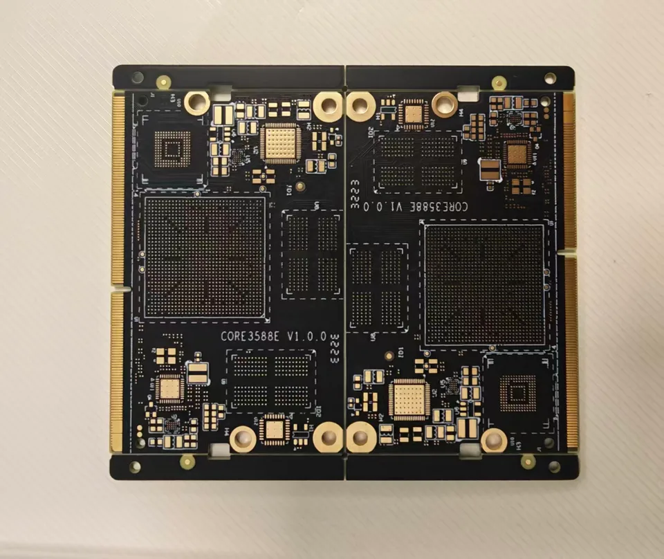
10-Layer High-Density PCB with 3.2/3.2 mil Fine Lines and Gold Fingers (10U76570)
JETFGO / 11

10-Layer High-Density PCB with 3.2/3.2 mil Fine Lines and Gold Fingers (10U76570)

A compact, high-density multilayer circuit board featuring complex BGA layouts, precision edge contacts and tightly controlled signal interconnections. Its combination of fine-pitch component footprints, advanced multilayer routing and specialized surface finishing demonstrates JETFGO's capabilities in manufacturing demanding embedded electronics PCBs.

ExpandCollapse
Product Model
10U76570
PCB Type
High-Density Multilayer Gold Finger PCB
Layer Count
10 Layers
More specificationsLess specifications
Base Material
FR-4 (S1000-2M)
Finished Board Thickness
1.20 mm
Finished Copper Weight
1 oz per Layer
Copper Stack-up
1/1/1/1/1/1/1/1/1/1
Minimum Trace Width
3.2 mil
Minimum Trace Spacing
3.2 mil
Minimum Hole Diameter
0.20 mm
Hole Aspect Ratio
6:1
Surface Finish
Immersion Gold + Electroplated Gold
Gold Finger Process
Selective Gold Plating
Connector Structure
PCB Edge Gold Fingers
BGA Layout
High-Density BGA Component Footprints
Impedance Control
Required
Impedance Control Groups
30
Solder Mask Color
Black
Silkscreen Color
White
Visible Board Marking
CORE3588E V1.0.0
Visible Brand Marking
MIXTILE
Key Manufacturing Processes
Fine-Line Etching, Multilayer Lamination, Controlled-Impedance Fabrication, Gold Finger Plating
Primary Manufacturing Challenges
Fine-Line Dimensional Control, Multilayer Registration, Dense BGA Routing and Multiple Impedance Requirements
View details
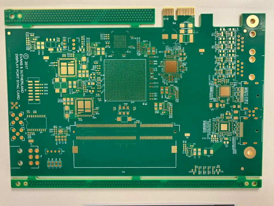
12-Layer Precision Gold Finger PCB with 4/4 mil Fine-Line Routing (12U52671)
JETFGO / 12

12-Layer Precision Gold Finger PCB with 4/4 mil Fine-Line Routing (12U52671)

A high-density multilayer circuit board featuring precision edge contacts, fine-pitch component layouts and complex circuit interconnections. Its combination of long and short gold fingers, selective plating and fine-line fabrication demonstrates JETFGO's capabilities in manufacturing advanced electronic interface boards.

ExpandCollapse
Product Model
12U52671
PCB Type
Precision Gold Finger Multilayer PCB
Layer Count
12 Layers
More specificationsLess specifications
Base Material
FR-4 (S1000-2M)
Finished Board Thickness
1.57 mm
Outer Layer Copper Weight
1 oz
Inner Layer Copper Weight
H (Engineering Stack-up Designation)
Copper Stack-up
1/H/H/H/H/H/H/H/H/H/H/1
Minimum Trace Width
4 mil
Minimum Trace Spacing
4 mil
Minimum Hole Diameter
0.20 mm
Hole Aspect Ratio
8:1
Surface Finish
Immersion Gold + Electroplated Gold
Special Plating Process
Selective Gold Electroplating
Gold Finger Configuration
Long and Short Gold Fingers
Gold Finger Plating Specification
51U (As Specified on Process Card)
Solder Mask Color
Green
Silkscreen Color
White
Connector Structure
PCB Edge Contacts
Visible Board Identification
Display Port Sync Card
Key Manufacturing Processes
Multilayer Lamination, Fine-Line Etching, Selective Gold Plating, Precision Gold Finger Fabrication
Primary Manufacturing Challenges
Multilayer Registration, Fine-Line Control, Gold Finger Dimensional Accuracy and Consistent Plating Quality
View details
12-Layer High-Density FR-4 PCB with Fine-Line Routing and ENIG
JETFGO / 13

12-Layer High-Density FR-4 PCB with Fine-Line Routing and ENIG

A compact, high-density multilayer circuit board featuring fine-pitch BGA connections, complex signal routing and densely arranged component pads. Its precision-fabricated interconnections demonstrate JETFGO's capabilities in multilayer registration, fine-line processing and controlled-impedance manufacturing.

ExpandCollapse
PCB Type
High-Density Multilayer PCB
Layer Count
12 Layers
Base Material
FR-4 (Shengyi S1000-2M)
More specificationsLess specifications
Glass Transition Temperature (Tg)
180°C
Finished Board Thickness
1.60 mm
Inner Layer Trace Width / Spacing
4 / 4 mil
Outer Layer Trace Width / Spacing
4 / 4 mil
Hole-to-Trace Clearance
8 mil
Minimum Hole Diameter
0.20 mm
Inner Layer Copper Weight
1 oz
Outer Layer Copper Weight
1 oz
Copper Stack-up
1 oz per Layer
Plated Hole Copper Thickness
18 μm
Surface Finish
ENIG (Electroless Nickel Immersion Gold)
Solder Mask Color
Green
Silkscreen Color
White
Impedance Control
Required
Impedance Control Groups
15
BGA Pad Structure
High-Density BGA Layout
SET Dimensions
79 × 62.16 mm
Drilled Hole Count
2,295
Test Points
3,631
Hole Density
467,353 Holes/m²
PCB Profiling
CNC Routing
Electrical Testing
Factory Flying Probe Test
View details
16-Layer High-Speed PCB with Precision Backdrilling and Fine-Line Routing (16C77908A0)
JETFGO / 14

16-Layer High-Speed PCB with Precision Backdrilling and Fine-Line Routing (16C77908A0)

A complex high-speed multilayer circuit board featuring dense component interconnections, precision backdrilled vias and tightly controlled fine-line circuitry. Its specialized fabrication processes demonstrate JETFGO's capabilities in advanced multilayer manufacturing, signal-path optimization and precision interconnection technology.

ExpandCollapse
Product Model
16C77908A0
PCB Type
High-Speed Multilayer PCB
Layer Count
16 Layers
More specificationsLess specifications
Base Material
Panasonic R5775G
Finished Board Thickness
2.20 mm
Outer Layer Copper Weight
1 oz
Inner Layer Copper Weight
0.5 oz
Minimum Trace Width
3 mil
Minimum Trace Spacing
3.3 mil
Minimum Hole Diameter
0.20 mm
Hole Aspect Ratio
11:1
BGA Feature Size
9.8 mil
Surface Finish
Immersion Gold (Engineering Confirmation Required)
Backdrilling Requirements
12 Backdrilling Groups
Backdrilling Accuracy
±2 mil
Backdrill-to-Trace Clearance
5.5 mil
Inner-Layer Hole-to-Trace Clearance
6 mil
Via Filling Process
Double-Sided Resin Plugging
Special Manufacturing Processes
Precision Backdrilling, Double-Sided Resin Via Plugging, Fine-Line Fabrication
Primary Manufacturing Challenges
Backdrilling Depth and Position Control, Tight Hole-to-Trace Clearance, Multilayer Registration and Resin Filling Consistency
View details
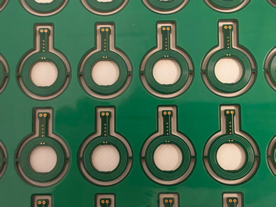
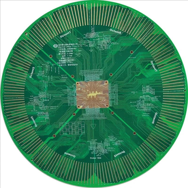
16-Layer Arlon 35N Multilayer Coil PCB with Blind and Buried Vias (16C76927A0)
JETFGO / 15

16-Layer Arlon 35N Multilayer Coil PCB with Blind and Buried Vias (16C76927A0)

A high-layer-count PCB featuring repeated circular coil structures and complex internal interconnections. Its manufacturing process combines multiple lamination cycles, precision hole formation and consistent copper patterning, demonstrating JETFGO's capability in specialized multilayer coil fabrication.

ExpandCollapse
Product Model
16C76927A0
PCB Type
High-Layer-Count Multilayer Coil PCB
Layer Count
16 Layers
More specificationsLess specifications
Base Material
Arlon 35N
Finished Board Thickness
2.70 mm
Inner Layer Copper Weight
2 oz
Outer Layer Copper Weight
2 oz
Minimum Trace Width
9.65 mil
Minimum Trace Spacing
7.5 mil
Minimum Hole Diameter
0.30 mm
Hole Aspect Ratio
9:1
Surface Finish
Immersion Gold (Pending Process Confirmation)
Special PCB Structure
Multilayer Circular Coil Patterns
Blind and Buried Via Structures
4 Groups
Lamination Process
5 Press Cycles
Circuit Pattern
Repeated Concentric Coil Layouts
Production Format
Multi-Unit Panelized Manufacturing
Key Manufacturing Processes
Multiple Lamination, Blind and Buried Via Formation, Precision Coil Patterning
Primary Manufacturing Challenges
Multilayer Registration, Lamination Alignment, Interlayer Connectivity and Copper Pattern Consistency
View details
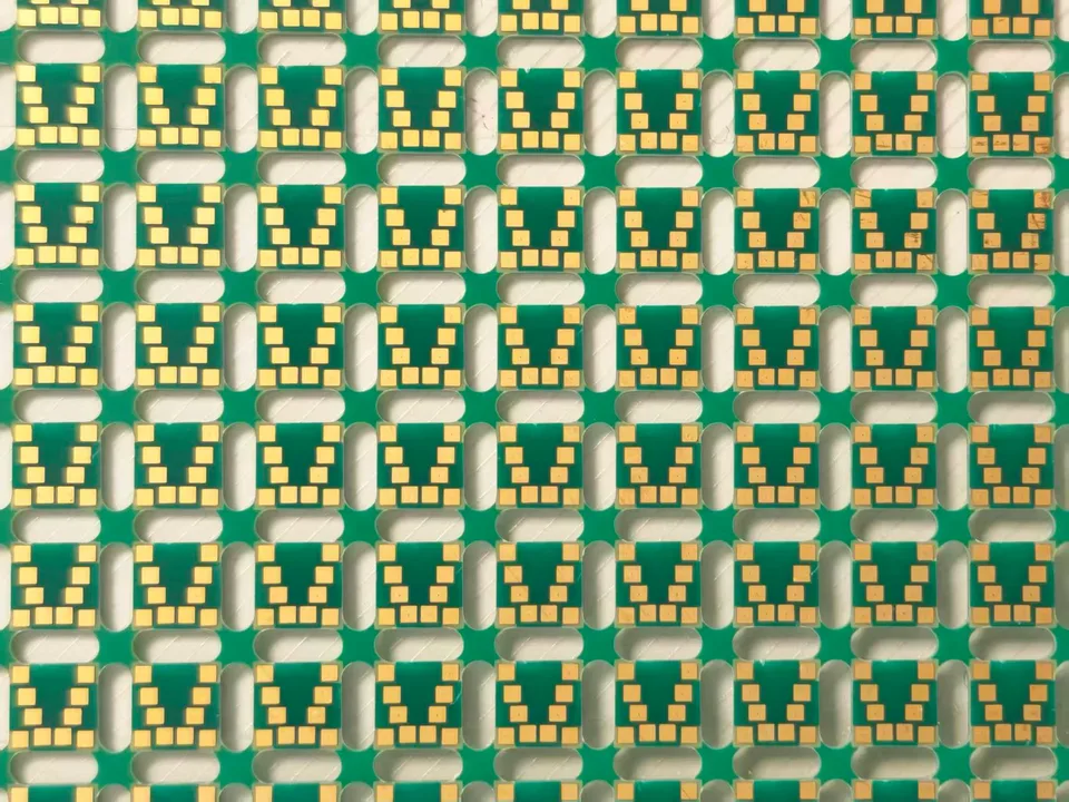
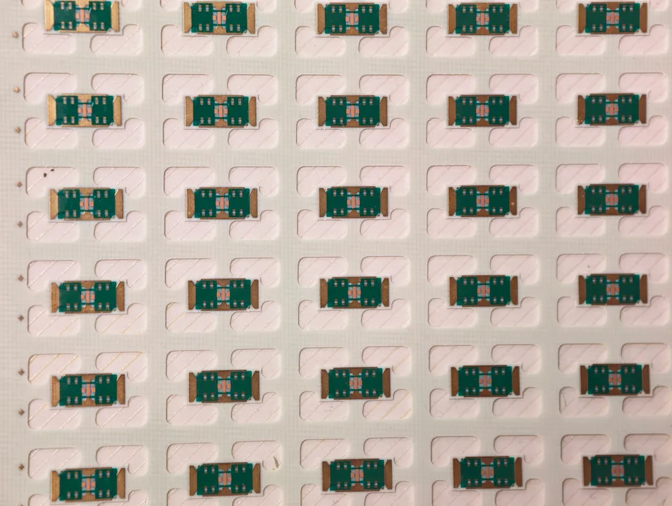
2-Layer Nickel-Free Soft Gold PCB with Precision Contact Pads (02D76828A0)
JETFGO / 16

2-Layer Nickel-Free Soft Gold PCB with Precision Contact Pads (02D76828A0)

A precision circuit board featuring repeated miniature contact-pad layouts and specialized gold-plated surfaces. The manufacturing process focuses on consistent pad geometry, controlled copper etching and uniform surface finishing across multiple PCB units.

ExpandCollapse
Product Model
02D76828A0
PCB Type
Nickel-Free Soft Gold PCB
Layer Count
2 Layers
More specificationsLess specifications
Base Material
KB-61610
Finished Board Thickness
1.20 mm
Finished Copper Weight
1 oz
Minimum Hole Diameter
0.20 mm
Hole Aspect Ratio
6:1
Surface Finish
Electroplated Gold
Special Gold Plating Process
Soft Gold Electroplating
Nickel-Free Plating
Yes
Gold Plating Coverage
Full-Board Nickel-Free Electrogold Process
Single-Side Lateral Etching Limit
≤25 μm
Solder Mask Color
Green
Contact Pad Structure
Repeated Miniature Gold-Plated Pads
Production Format
Multi-Unit PCB Panelization
Key Manufacturing Processes
Nickel-Free Gold Electroplating, Soft Gold Finishing, Precision Copper Etching
Primary Manufacturing Challenges
Nickel-Free Gold Plating and Lateral Etching Control
View details
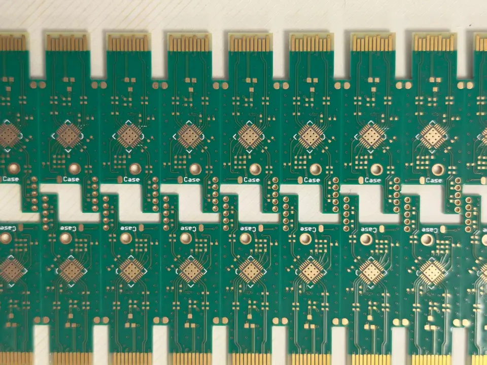
4-Layer Precision Gold Finger PCB with Selective Gold Plating (04U76379A0)
JETFGO / 17

4-Layer Precision Gold Finger PCB with Selective Gold Plating (04U76379A0)

A precision edge-connector PCB featuring multiple gold-plated contact fingers, fine-pitch circuitry and customized panelization. The manufacturing process emphasizes consistent contact geometry, clean plating boundaries and accurate dimensional control for reliable electronic interconnections.

ExpandCollapse
Product Model
04U76379A0
PCB Type
Precision Gold Finger PCB
Layer Count
4 Layers
More specificationsLess specifications
Base Material
KB-6160
Finished Board Thickness
1.0 mm
Inner Layer Copper Weight
1 oz
Outer Layer Copper Weight
1 oz
Minimum Trace Width
5 mil
Minimum Trace Spacing
5 mil
Minimum Hole Diameter
0.30 mm
Hole Aspect Ratio
3.3:1
Surface Finish
Immersion Gold + Electroplated Gold
Special Plating Process
Selective Gold Electroplating
Connector Contact Type
Gold Fingers
Gold Finger Configuration
Long and Short Contact Fingers
Gold Finger-to-Board-Edge Distance Tolerance
±0.05 mm
Gold Finger End Requirement
Flat, Residue-Free Finish
Solder Mask Color
Green
Silkscreen Color
White
Production Format
Multi-Unit Panelization
Key Manufacturing Processes
Selective Gold Plating, Fine-Line Etching, Precision Edge Contact Fabrication
Primary Manufacturing Challenges
Gold Finger End Quality, Plating Residue Control and Contact Position Accuracy
View details
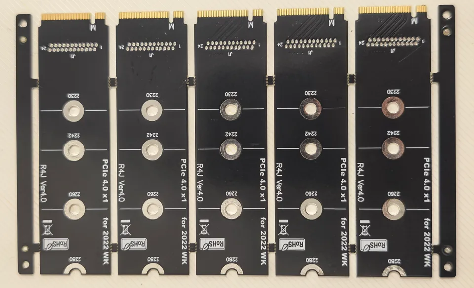
2-Layer PCIe 4.0 x1 Gold Finger PCB with Selective Gold Plating (02K76422A0)
JETFGO / 18

2-Layer PCIe 4.0 x1 Gold Finger PCB with Selective Gold Plating (02K76422A0)

A compact edge-connector circuit board featuring precision-fabricated gold fingers, dedicated mounting holes and a combination of surface finishing processes. This manufacturing example highlights contact-area plating quality, edge-connector finishing and dimensional consistency for electronic interface applications.
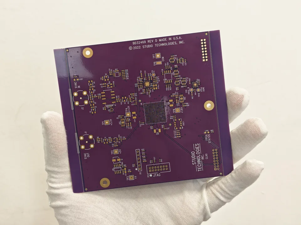
ExpandCollapse
Product Model
02K76422A0
PCB Type
PCIe Edge Connector PCB
Layer Count
2 Layers
More specificationsLess specifications
Base Material
FR-4 (S1000-2M)
Finished Board Thickness
0.80 mm
Finished Copper Weight
1 oz
Minimum Trace Width
6 mil
Minimum Trace Spacing
5.1 mil
Minimum Hole Diameter
0.30 mm
Hole Aspect Ratio
2.67:1
Surface Finish
Lead-Free HASL + Electroplated Gold
Special Plating Process
Selective Gold Plating
Connector Contact Type
Gold Fingers
Gold Finger Process
Localized Electroplated Gold
Gold Finger Quality Requirement
Flat and Residue-Free Contact Ends
Solder Mask Color
Black
Silkscreen Color
White
Visible Interface Marking
PCIe 4.0 x1
Key Manufacturing Capabilities
Gold Finger Plating, Selective Surface Finishing and Contact Edge Quality Control
Primary Manufacturing Challenge
Gold Finger End Flatness and Residue Prevention
View details
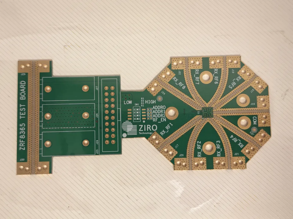
4-Layer Taconic TSM-DS3 Hybrid RF PCB with Edge Plating (04C73460A0)
JETFGO / 19

4-Layer Taconic TSM-DS3 Hybrid RF PCB with Edge Plating (04C73460A0)

A specialized RF circuit board combining high-frequency laminate materials with conventional multilayer construction. Its radial signal-routing layout, multiple RF connection points and precision-fabricated copper features demonstrate JETFGO's capabilities in complex hybrid-material PCB manufacturing.
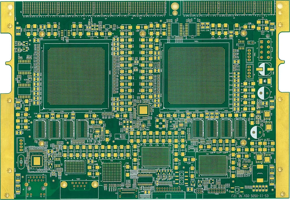
ExpandCollapse
Product Model
04C73460A0
PCB Type
Hybrid-Material RF PCB
Layer Count
4 Layers
More specificationsLess specifications
Base Materials
Taconic TSM-DS3 + S1000-2M
Laminate Construction
Mixed-Dielectric Hybrid Lamination
Finished Board Thickness
1.60 mm
Inner Layer Copper Weight
1 oz
Outer Layer Copper Weight
1.5 oz
Minimum Trace Width
4 mil
Minimum Trace Spacing
5.5 mil
Minimum Hole Diameter
0.175 mm
Hole Aspect Ratio
9.14:1
BGA Feature Size
0.18 mm
Surface Finish
Immersion Gold
Via Filling Process
Resin Plugging
Edge Treatment
Metal Edge Plating
Signal Trace Tolerance
±15 μm
BGA Feature Tolerance
±10%
Surface Copper Tolerance
±5 μm
Key Manufacturing Processes
Hybrid Lamination, Fine-Line Etching, Resin Via Plugging, Edge Metallization
Primary Technical Challenges
Material Compatibility, Precise RF Trace Dimensions, Copper Thickness Control and Fine-Pitch Processing
View details
2-Layer Rogers RO4350B Ultra-Thin PCB with Laser-Drilled Holes (02N76257A0)
JETFGO / 20

2-Layer Rogers RO4350B Ultra-Thin PCB with Laser-Drilled Holes (02N76257A0)

A precision high-frequency laminate PCB featuring an ultra-thin construction, fine-pitch circuitry and specialized plated-hole filling. Its combination of advanced material processing and surface finishing demonstrates JETFGO's capability to manufacture delicate, high-precision circuit boards with demanding fabrication requirements.
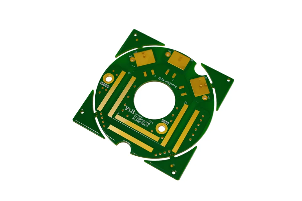
ExpandCollapse
Product Model
02N76257A0
PCB Type
Thin High-Frequency Laminate PCB
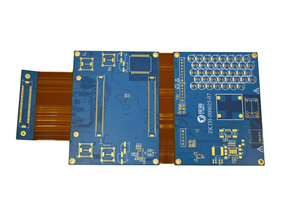
Layer Count
2 Layers
More specificationsLess specifications
Base Material
Rogers RO4350B
Finished Board Thickness
0.30 mm
Finished Copper Weight
1 oz
Minimum Trace Width
4 mil
Minimum Trace Spacing
4.3 mil
Minimum Hole Diameter
0.10 mm
Hole Aspect Ratio
3:1
Drilling Technology
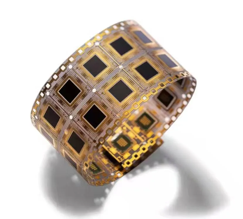
Laser Through-Hole Drilling
Special Hole Process
Plated-Hole Filling
Surface Finish
ENIG + OSP
Manufacturing Challenge
Thin-Board Handling and Breakage Prevention
Fine-Line Process Challenge
2.7 mil Spacing After Compensation
Electroplating Challenge
Fine-Line Photoresist Pinching Risk
Key Manufacturing Capability
Precision Laser Drilling, Hole Plating and Filling
Production Format
Multi-Unit Panelization
View details
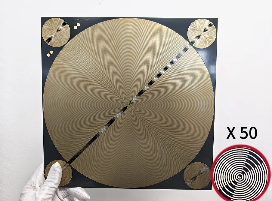
Fine-Line Coil PCB with 3/3 mil Traces, ENIG Finish and Clear Conformal Coating
JETFGO / 21

Fine-Line Coil PCB with 3/3 mil Traces, ENIG Finish and Clear Conformal Coating

A precision coil PCB featuring a large-area spiral circuit pattern, 3/3 mil trace width and spacing, ENIG surface finish, and transparent conformal coating. A demonstration of fine-line PCB fabrication and surface protection capabilities.

ExpandCollapse
Circuit Structure
Large-Area Spiral Coil
Trace Width
3 mil
Trace Spacing
3 mil
More specificationsLess specifications
Surface Finish
ENIG (Electroless Nickel Immersion Gold)
Protective Coating
Transparent Conformal Coating (Spray Applied)
Key Manufacturing Process
Fine-Line Coil Circuit Fabrication
View details
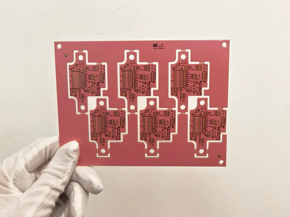
4-Layer FR-4 PCB with Pink Solder Mask and ENIG Finish (130969)
JETFGO / 22

4-Layer FR-4 PCB with Pink Solder Mask and ENIG Finish (130969)

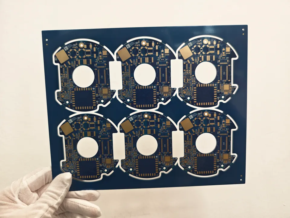
A customized 4-layer FR-4 PCB featuring KB-6167F TG170 material, 1.575 mm thickness, 8/8 mil trace width and spacing, pink solder mask, black silkscreen and ENIG surface finish. Designed with a 3 × 2 panel layout for efficient multi-unit PCB manufacturing.

ExpandCollapse
Layer Count
4 Layers
Base Material
FR-4 (KB-6167F)
Glass Transition Temperature (Tg)
170°C
More specificationsLess specifications
Board Thickness
1.575 mm
Inner Layer Trace Width / Spacing
8 / 8 mil
Outer Layer Trace Width / Spacing
8 / 8 mil
Hole-to-Trace Clearance
8 mil
Minimum Hole Diameter
0.20 mm
Inner Copper Weight
1 oz
Outer Copper Weight
1 oz
Copper Stack-up
1/1/1/1 oz
Hole Copper Thickness
20 μm
Surface Finish
ENIG (Electroless Nickel Immersion Gold)
Gold Thickness
2 μin
Nickel Thickness
120 μin
Solder Mask Color
Pink
Silkscreen Color
Black
Silkscreen Ink Model
Guangxin KSM-388BK+
Panelization
3 × 2 (6 Units per Panel)
Panel Dimensions
146.35 × 110.06 mm
Panel Hole Count
1,100
Total Hole Count
1,466
Hole Density
68,293 holes/m²
Via Process
According to Design Files
Manufacturing Method
CNC Routing
Testing Method
Factory Flying Probe Test
View details
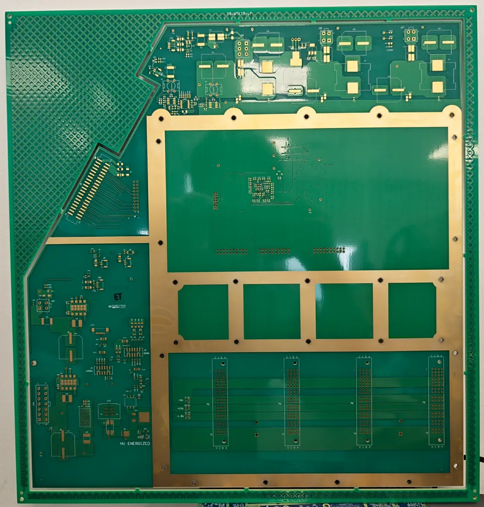
6-Layer Fine-Line Multilayer PCB with ENIG Finish (114340)
JETFGO / 23

6-Layer Fine-Line Multilayer PCB with ENIG Finish (114340)

A 6-layer FR-4 multilayer PCB manufactured with S1000-2M TG180 material, featuring 2.36 mm board thickness, fine-line circuitry, 0.5 oz inner copper, 1.5 oz outer copper, green solder mask and ENIG surface finish.

ExpandCollapse
Layer Count
6 Layers
Base Material
FR-4 (S1000-2M)
Glass Transition Temperature (Tg)
180°C
More specificationsLess specifications
Board Thickness
2.36 mm
Board Thickness Tolerance
±10%
Inner Layer Trace Width / Spacing
3.94 / 5 mil
Outer Layer Trace Width / Spacing
4.92 / 5 mil
Hole-to-Trace Clearance
8 mil
Minimum Hole Diameter
0.25 mm
Inner Copper Weight
0.5 oz
Outer Copper Weight
1.5 oz
Copper Stack-up
1.5/H/H/H/H/1.5
Hole Copper Thickness
20 μm
Surface Finish
ENIG (Electroless Nickel Immersion Gold)
Gold Thickness
2 μin
Nickel Thickness
120 μin
Solder Mask Color
Green
Solder Mask Coverage
Double-Sided
Solder Mask Model
KSM-S61
Silkscreen Color
White
Silkscreen Coverage
Double-Sided
PCB Dimensions
345 × 367.3 mm
SET Dimensions
370.4 × 392.7 mm
Panelization
1 × 1
Drilled Hole Count
1,623
Test Points
1,937
Hole Density
11,159 holes/m²
Via Process
According to Design Files
Manufacturing Method
CNC Routing
Testing Method
Factory Flying Probe Test
View details
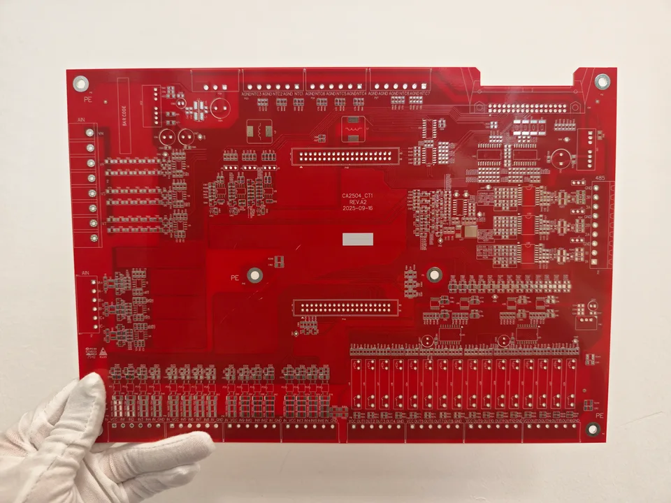
4-Layer Industrial Control PCB with Red Solder Mask (115370)
JETFGO / 24

4-Layer Industrial Control PCB with Red Solder Mask (115370)

A 4-layer FR-4 PCB featuring KB-6165F TG150 material, 5/5 mil trace width and spacing, 1.6 mm thickness, red solder mask, white silkscreen and lead-free HASL surface finish. Manufactured for customized industrial electronic control applications.

ExpandCollapse
Layer Count
4 Layers
Base Material
FR-4 (KB-6165F)
Glass Transition Temperature (Tg)
150°C
More specificationsLess specifications
Board Thickness
1.6 mm
Inner Layer Trace Width / Spacing
5 / 5 mil
Outer Layer Trace Width / Spacing
5 / 5 mil
Hole-to-Trace Clearance
8 mil
Minimum Hole Diameter
0.20 mm
Inner Copper Weight
1 oz
Outer Copper Weight
1 oz
Copper Stack-up
1/1/1/1 oz
Hole Copper Thickness
25 μm
Surface Finish
Lead-Free HASL
Solder Mask Color
Red
Solder Mask Model
KSM-S61
Silkscreen Color
White
Panel Dimensions
300 × 209.9 mm
Panelization
1 × 1
Drilled Hole Count
1,580
Test Points
2,689
Hole Density
25,092 holes/m²
Via Process
According to Design Files
Manufacturing Method
CNC Routing
Testing Method
Customer-Specified Flying Probe Test
View details
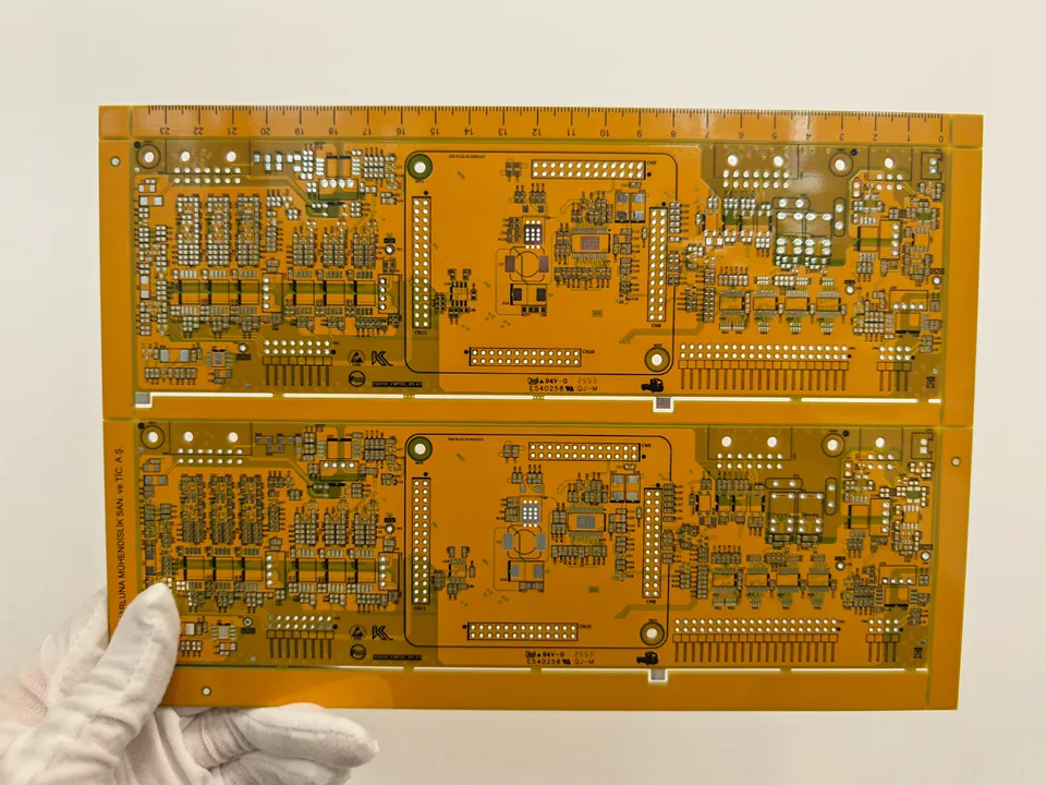
6-Layer Multilayer PCB with Yellow Solder Mask and TG150 Material (119728)
JETFGO / 25

6-Layer Multilayer PCB with Yellow Solder Mask and TG150 Material (119728)

A 6-layer FR-4 PCB manufactured with KB-6165GC TG150 material, featuring 10/8 mil trace width and spacing, 1.6 mm board thickness, yellow solder mask, black silkscreen and lead-free HASL surface finish. Suitable for customized multilayer electronic circuit applications.

ExpandCollapse
Layer Count
6 Layers
Base Material
FR-4 (KB-6165GC)
Glass Transition Temperature (Tg)
150°C
More specificationsLess specifications
Board Thickness
1.6 mm
Inner Layer Trace Width / Spacing
10 / 8 mil
Outer Layer Trace Width / Spacing
10 / 8 mil
Hole-to-Trace Clearance
7.87 mil
Minimum Hole Diameter
0.30 mm
Inner Copper Weight
1 oz
Outer Copper Weight
1 oz
Copper Stack-up
1/1/1/1/1/1 oz
Hole Copper Thickness
20 μm
Surface Finish
Lead-Free HASL
Solder Mask Color
Yellow
Solder Mask Model
KSM-S61
Silkscreen Color
Black
Panel Dimensions
263.2 × 182.18 mm
Panelization
2 × 1
SET Drill Count
1,814
Total Drill Count
3,034
Hole Density
37,832 holes/m²
Via Process
According to Design Files
Manufacturing Method
CNC Routing
Testing Method
Factory Flying Probe Test
View details
12-Layer Impedance-Controlled Multilayer PCB with TG180 Material and ENIG Finish (114533)
JETFGO / 26

12-Layer Impedance-Controlled Multilayer PCB with TG180 Material and ENIG Finish (114533)

A 12-layer FR-4 multilayer PCB featuring TG180 S1000-2M material, 5/5 mil fine-line circuitry, 27 impedance control groups and ENIG surface finish. Designed for complex electronic systems requiring reliable signal transmission and high-density circuit integration.

ExpandCollapse
Layer Count
12 Layers
Base Material
FR-4 (S1000-2M)
Glass Transition Temperature (Tg)
180°C
More specificationsLess specifications
Board Thickness
1.575 mm
Inner Layer Trace Width / Spacing
5 / 5 mil
Outer Layer Trace Width / Spacing
5 / 5 mil
Hole-to-Trace Clearance
8 mil
Minimum Hole Diameter
0.20 mm
Inner Copper Weight
1 oz
Outer Copper Weight
1 oz
Copper Stack-up
1 oz per layer (12-layer construction)
Hole Copper Thickness
20 μm
Surface Finish
ENIG (Electroless Nickel Immersion Gold)
Gold Thickness
2 μin
Solder Mask
Double-Sided
Solder Mask Color
Green
Silkscreen Color
White
SET Dimensions
365.76 × 149.23 mm
Panelization
1 × 1
Number of Drilled Holes
3,292
Test Points
4,850
Impedance Control
Yes
Impedance Control Groups
27
Via Process
Aluminum Sheet Via Plugging
Manufacturing Method
CNC Routing
Testing Method
Customer Flying Probe Test
View details
8-Layer High-Density Multilayer PCB with Blue Solder Mask and ENIG Finish (115063)
JETFGO / 27

8-Layer High-Density Multilayer PCB with Blue Solder Mask and ENIG Finish (115063)

An 8-layer FR-4 multilayer PCB featuring TG170 material, 4/4 mil fine-line circuitry, blue solder mask and ENIG surface finish. Manufactured with customized panelization and via plugging processes for complex electronic assemblies.

ExpandCollapse
Layer Count
8 Layers
Base Material
FR-4 (Kingboard KB-6167F)
Glass Transition Temperature (Tg)
170°C
More specificationsLess specifications
Board Thickness
1.6 mm
Inner Layer Trace Width / Spacing
4 / 4 mil
Outer Layer Trace Width / Spacing
4 / 4 mil
Hole-to-Trace Clearance
8 mil
Minimum Hole Diameter
0.20 mm
Inner Copper Weight
1 oz
Outer Copper Weight
1 oz
Copper Stack-up
1 / 1 / 1 / 1 / 1 / 1 / 1 / 1 oz
Hole Copper Thickness
25 μm
Surface Finish
ENIG (Electroless Nickel Immersion Gold)
Gold Thickness
2 μin
Solder Mask
Double-Sided
Solder Mask Color
Blue
Silkscreen Color
White
Panelization
3 × 2 (6 PCBs per panel)
Panel Dimensions
223.75 × 180.42 mm
Drilled Holes per PCB
1,100
Total Drilled Holes per Panel
6,600
Test Points per PCB
702
Total Test Points per Panel
4,212
Impedance Control
Yes
Via Process
Aluminum Sheet Via Plugging
Manufacturing Method
CNC Routing
Testing Method
Factory Flying Probe Test
Acceptance Standard
IPC-A-600 Class 3
View details
12-Layer High-TG Multilayer PCB with Controlled Impedance and ENIG Finish (114630)
JETFGO / 28

12-Layer High-TG Multilayer PCB with Controlled Impedance and ENIG Finish (114630)

A 12-layer FR-4 multilayer PCB manufactured with TG180 S1000-2M material, featuring 6/6 mil trace width and spacing, 2.0 mm board thickness, controlled impedance and ENIG surface finish. Designed for complex electronic circuit integration and demanding signal transmission requirements.

ExpandCollapse
Layer Count
12 Layers
Base Material
FR-4 (S1000-2M)
Glass Transition Temperature (Tg)
180°C
More specificationsLess specifications
Board Thickness
2.0 mm
Inner Layer Trace Width / Spacing
6 / 6 mil
Outer Layer Trace Width / Spacing
6 / 6 mil
Hole-to-Trace Clearance
8 mil
Minimum Hole Diameter
0.25 mm
Inner Copper Weight
1 oz
Outer Copper Weight
1 oz
Copper Stack-up
1 oz copper layers (12-layer construction)
Hole Copper Thickness
18 μm
Surface Finish
ENIG (Electroless Nickel Immersion Gold)
Gold Thickness
1.5 μin
Solder Mask Color
Green
Silkscreen Color
White
Board / Set Dimensions
229.5 × 149 mm
Number of Drilled Holes
2,280
Test Points
3,218
Impedance Control
Yes
Impedance Groups
10
Via Process
Via Tenting
Manufacturing Method
CNC Routing
Testing Method
Factory Flying Probe Test
View details
4-Layer Custom Ring-Shaped PCB with White Solder Mask and ENIG Finish (100942)
JETFGO / 29

4-Layer Custom Ring-Shaped PCB with White Solder Mask and ENIG Finish (100942)

A custom-shaped multilayer PCB featuring a circular structure, double-sided white solder mask and ENIG surface finish. Suitable for electronic assemblies requiring specialized mechanical layouts and reliable electrical connections.

ExpandCollapse
Layer Count
4 Layers
Base Material
FR-4 (Kingboard KB-6164)
Glass Transition Temperature (Tg)
140°C
More specificationsLess specifications
Board Thickness
1.0 mm
Board Thickness Tolerance
±0.1 mm
Inner Layer Trace Width / Spacing
8 / 8 mil
Outer Layer Trace Width / Spacing
8 / 8 mil
Hole-to-Trace Clearance
8 mil
Minimum Hole Diameter
0.25 mm
Inner Copper Weight
1 oz
Outer Copper Weight
1 oz
Copper Stack-up
1 / 1 / 1 / 1 oz
Hole Copper Thickness
20 μm
Surface Finish
ENIG (Electroless Nickel Immersion Gold)
Solder Mask
Double-Sided
Solder Mask Color
White
Silkscreen
None
PCB Dimensions
230 × 230 mm
Production Set Dimensions
250 × 250 mm
Number of Drilled Holes
930
Test Points
1,404
Routing Method
CNC Routing
Via Process
According to Design Files
View details
6-Layer TG170 FR-4 High-Density PCB with 4/4 mil Fine-Line Routing and ENIG (68000)
JETFGO / 30

6-Layer TG170 FR-4 High-Density PCB with 4/4 mil Fine-Line Routing and ENIG (68000)

A high-density multilayer circuit board featuring intricate component layouts, fine-pitch connections and multiple controlled-impedance requirements. Developed for complex electronic systems requiring precise circuit integration and reliable electrical performance.

ExpandCollapse
Layer Count
6 Layers
Base Material
FR-4 (Kingboard KB-6167F)
Glass Transition Temperature (Tg)
170°C
More specificationsLess specifications
Board Thickness
1.27 mm
Inner Layer Trace Width / Spacing
4 / 4 mil
Outer Layer Trace Width / Spacing
4 / 4 mil
Hole-to-Trace Clearance
8 mil
Minimum Hole Diameter
0.25 mm
Inner Copper Weight
1 oz
Outer Copper Weight
1 oz
Copper Stack-up
1 / 1 / 1 / 1 / 1 / 1 oz
Hole Copper Thickness
20 μm
Surface Finish
ENIG (Electroless Nickel Immersion Gold)
Solder Mask Color
Blue
Silkscreen Color
White
Impedance Control
Required (11 impedance groups)
Panel Dimensions
180 × 135 mm
Number of Drilled Holes
4,537
Test Points
4,400
View details
6-Layer TG180 FR-4 PCB with Fine-Line Routing and ENIG (58998)
JETFGO / 31

6-Layer TG180 FR-4 PCB with Fine-Line Routing and ENIG (58998)

A compact multilayer PCB featuring dense component placement, fine-line circuitry and multiple interface connections. Designed for electronic systems requiring reliable signal management, synchronization and stable control performance.

ExpandCollapse
Layer Count
6 Layers
Base Material
FR-4 (S1000-2M)
Glass Transition Temperature (Tg)
180°C
More specificationsLess specifications
Board Thickness
1.6 mm
Inner Layer Trace Width / Spacing
5 / 5 mil
Outer Layer Trace Width / Spacing
5 / 5 mil
Hole-to-Trace Clearance
8 mil
Minimum Hole Diameter
0.20 mm
Inner Copper Weight
0.5 oz
Outer Copper Weight
1.5 oz
Copper Stack-up
1.5 / 0.5 / 0.5 / 0.5 / 0.5 / 1.5 oz
Hole Copper Thickness
25 μm
Surface Finish
ENIG (Electroless Nickel Immersion Gold)
Gold Thickness
3 μin
Nickel Thickness
120 μin
Solder Mask Color
Purple
Silkscreen Color
White
Impedance Control
Required (5 impedance groups)
Board Dimensions
104.14 × 116.84 mm
Number of Drilled Holes
492
Test Points
909
View details
12-Layer High-Tg FR-4 PCB with 2 oz Copper and ENIG (124406)
JETFGO / 32

12-Layer High-Tg FR-4 PCB with 2 oz Copper and ENIG (124406)

A complex multilayer PCB featuring fine-pitch circuitry and large power connection pads, developed to support demanding electronic assemblies. Its construction provides a manufacturing reference for applications requiring reliable electrical connections, thermal stability and integration of control and power circuits.

ExpandCollapse
PCB Type
Rigid Multilayer PCB
Layer Count
12 Layers
Base Material
FR-4
More specificationsLess specifications
Material Manufacturer
Shengyi
Laminate Grade
S1000-2M
Glass Transition Temperature (Tg)
180°C
Finished Board Thickness
2.94 mm
Inner-Layer Copper Weight
2 oz
Outer-Layer Copper Weight
2 oz
Inner-Layer Trace Width / Spacing
7 / 8 mil
Outer-Layer Trace Width / Spacing
7 / 8 mil
Hole-to-Trace Clearance
8 mil
Minimum Hole Diameter
0.20 mm
Plated Hole Copper Thickness
20 μm
Surface Finish
ENIG (Electroless Nickel Immersion Gold)
Solder Mask
Green
Silkscreen
White
Panel Size
94 × 77 mm
Panelization
1 × 2
Board Profiling
CNC Routing
View details
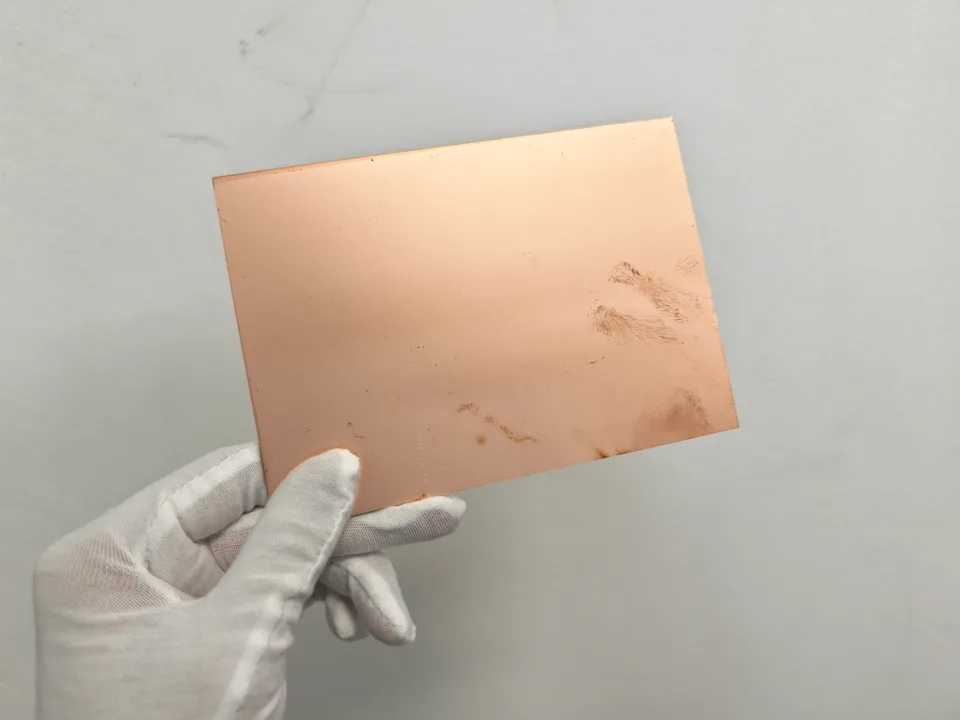
Standard PCB Base Material Panel
JETFGO / 33

Standard PCB Base Material Panel

A standard PCB base material panel with an unpatterned copper-colored surface, shown before circuit fabrication. This material reference illustrates the starting stage of PCB manufacturing, before processes such as circuit patterning, drilling, etching and surface finishing.

ExpandCollapse
Material Type
Copper-Clad Laminate (CCL)
Base Material Options
FR-4, High-Tg FR-4, Halogen-Free Laminates
FR-4 Material Grades
Tg135, Tg150, Tg170, Tg180
More specificationsLess specifications
Material Suppliers
Shengyi, ITEQ, KB, EMC
Rigid PCB Layer Count
Up to 60 Layers
Rigid PCB Thickness Range
0.3–8.0 mm
Inner-Layer Copper Weight
1/3–28 oz
Outer-Layer Copper Weight
1/3–28 oz
Minimum Trace Width / Spacing
3 / 2.5 mil
Minimum Finished PCB Size
10 × 10 mm
Controlled Impedance Tolerance
±8%
Mechanical Drilling Aspect Ratio
Up to 20:1
Laser-Drilled Microvia Diameter
3–5 mil
Available Surface Finishes
HASL, Lead-Free HASL, OSP, ENIG, ENEPIG, Immersion Silver, Immersion Tin, Gold Plating
Solder Mask Options
Green, Black, White, Blue, Red, Yellow, Purple, Gray
Manufacturing Services
PCB Prototyping, Multilayer Fabrication, Small-Batch and Volume Production
Engineering Review
Material Availability, Copper Thickness, Stackup and Process Feasibility Subject to Confirmation
View details
JETFGO / Products

PCB Manufacturing Categories

15
Conventional PCB Manufacturer
01

Conventional PCB Manufacturer

Single-sided, double-sided and multilayer PCBs are fabricated to customer specifications for industrial, communications, computing and medical electronics. JETFGO supports prototypes and production orders from its Shenzhen factory.

ExpandCollapse
View details
HDI PCB Manufacturer
02

HDI PCB Manufacturer

HDI PCBs use laser microvias, sequential lamination and fine-line routing to connect dense electronic designs. JETFGO manufactures custom HDI boards for prototypes, NPI and volume production.

ExpandCollapse
View details
High Frequency PCB Manufacturer
03

High Frequency PCB Manufacturer

High-frequency RF PCBs use low-loss laminates and controlled impedance for communication, radar and microwave circuits. JETFGO reviews materials and stack-ups before custom fabrication.

ExpandCollapse
View details
High Speed PCB Manufacturer
04

High Speed PCB Manufacturer

High-speed PCBs use low-loss materials and controlled impedance to support signal integrity in digital computing and data-communication systems. JETFGO fabricates customer-designed boards after stack-up review.

ExpandCollapse
View details
Hybrid PCB Manufacturer
05

Hybrid PCB Manufacturer

Hybrid PCBs combine RF laminates and FR-4 within one board for applications needing different electrical material properties. JETFGO reviews mixed-material stack-ups for high-frequency and high-speed projects before fabrication.

ExpandCollapse
View details
Rigid-Flex PCB Manufacturer
06

Rigid-Flex PCB Manufacturer

Rigid-flex PCBs combine rigid board sections and flexible circuits in one structure for compact electronics and complex interconnections. JETFGO reviews the layer stack-up and materials before custom fabrication.

ExpandCollapse
View details
Flexible PCB Manufacturer
07

Flexible PCB Manufacturer

Flexible PCBs use polyimide materials and fine-feature circuits for compact electronics that need bendable interconnections. JETFGO supports custom flex-board projects from prototype through volume production.

ExpandCollapse
View details
Metal Base PCB Manufacturer
08

Metal Base PCB Manufacturer

Metal-base PCBs use aluminum or copper substrates to manage heat in power electronics and other demanding assemblies. JETFGO reviews materials, thermal performance and layer structure before fabrication.

ExpandCollapse
View details
Multilayer PCB Manufacturer
09

Multilayer PCB Manufacturer

Multilayer PCB manufacturing with advanced layer structures, engineering support, prototype capability and scalable production for industrial electronics.

ExpandCollapse
View details
Copper Inlay PCB Manufacturer
10

Copper Inlay PCB Manufacturer

Copper inlay PCB manufacturing with embedded copper inserts for direct thermal management in high-power, automotive and industrial electronic applications.

ExpandCollapse
View details
ABF IC Substrate Manufacturing Capability
12

ABF IC Substrate Manufacturing Capability

ABF (Ajinomoto Build-up Film) IC package substrates provide fine-line interconnections for advanced semiconductor packaging. JETFGO reviews laser microvias, any-layer build-up and SAP/mSAP requirements before confirming project feasibility.

ExpandCollapse
View details
Special Technology PCB Manufacturing
13

Special Technology PCB Manufacturing

Specialty PCBs are a category of custom boards, including heavy-copper, thermoelectric-separation, extra-thick, extra-long and reinforced structures for power, thermal and industrial applications. Each design receives engineering review before production.

ExpandCollapse
View details
PCB ENGINEERING LIBRARY

PCB Manufacturing Guides & Technical Resources

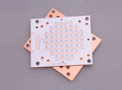
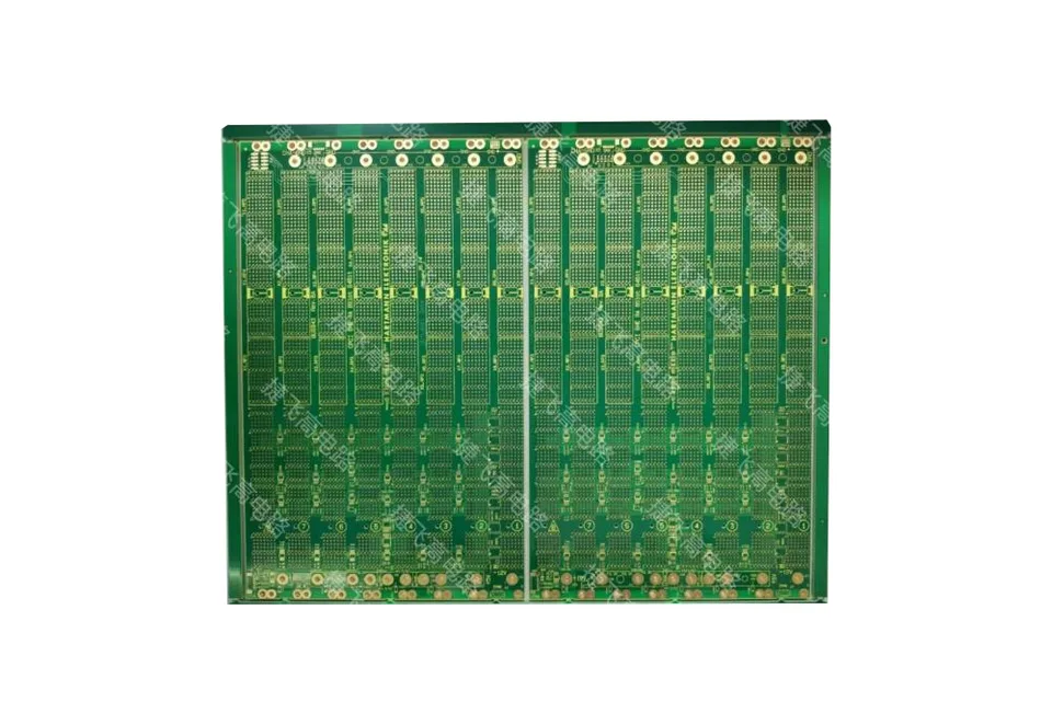
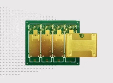
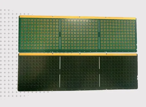
Explore JETFGO's PCB manufacturing technologies, product examples, process capabilities, factory equipment and quality systems to support PCB and PCBA sourcing decisions.

JETFGO / PCB33 Reference
Product & factory gallery
PCB ENGINEERING LIBRARY
Engineering library
RFQ / DFM

Discuss your next order directly with our factory.

Send the Gerber or ODB++, stackup, material, quantity, target date and test requirements. Our team will review feasibility and return a technical quotation for the order you manage.

Engineering reviewMaterial & stackupPrecision fabrication
Contact Us